Check patentability & draft patents in minutes with Patsnap Eureka AI!

Solid-state structure comprising a battery and a variable resistor of which the resistance is controlled by variation of the concentration of active species in electrodes of the battery

Inactive Publication Date: 2010-01-07
KONINKLIJKE PHILIPS ELECTRONICS NV
View PDF2 Cites 8 Cited by
  • Summary
  • Abstract
  • Description
  • Claims
  • Application Information

AI Technical Summary

Benefits of technology

[0029]The invention also provides an electrical device comprising a controllable resistor as claimed in any of the preceding claims. Also in such an embodiment the fruitful effects of the invention appear very well.
[0030]The invention also provides a method for producing a solid-state variable resistor, comprising a first battery electrode layer deposited on a substrate, a solid electrolyte layer deposited on said first battery electrode layer, a second battery electrode layer deposited on the solid electrolyte layer, two resistor contacts being both in contact with one of the electrode layers, wherein the method comprises the steps of deposition of the first electrode layer on the substrate, deposition of a solid electrolyte layer on the first electrode layer, deposition of a second electrode layer on the solid electrolyte layer, deposition of a pair of electrodes, wherein the electrodes are deposited either preceding or following the deposition of one of the electrode layers. Through this method the resistor according to the invention is produced in a simple and effective way. An important feature of the resistor of the invention is formed by the presence of the resistor contacts, required to form the resistor circuit. These contacts can be deposited after the deposition of the electrode layer through which the path between the contacts extends. In this situation the electrodes are within the volume of the electrolyte layer in contact with the electrode layer.
[0031]However it is also possible that the contacts are deposited before the electrode layer is deposited. In that case contact between a current collector layer and the contacts should be avoided. Consequently a preferred method comprises the steps of deposition of an anodic electrode layer on the substrate, deposition of a pair of contacts on the anodic layer, deposition of a solid electrolyte layer on the anodic layer and on the contacts and deposition of a cathodic electrode layer on said electrolyte layer.

Problems solved by technology

Secondly, as the electrochemical doping of the material that serves as the conducting pathway is fully reversible, almost no power is dissipated (as heat) in tuning the resistance thereof.

Method used


Image

  • Solid-state structure comprising a battery and a variable resistor of which the resistance is controlled by variation of the concentration of active species in electrodes of the battery
  • Solid-state structure comprising a battery and a variable resistor of which the resistance is controlled by variation of the concentration of active species in electrodes of the battery
  • Solid-state structure comprising a battery and a variable resistor of which the resistance is controlled by variation of the concentration of active species in electrodes of the battery

Examples


Embodiment Construction

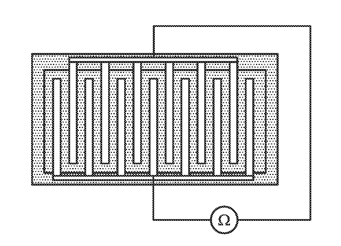
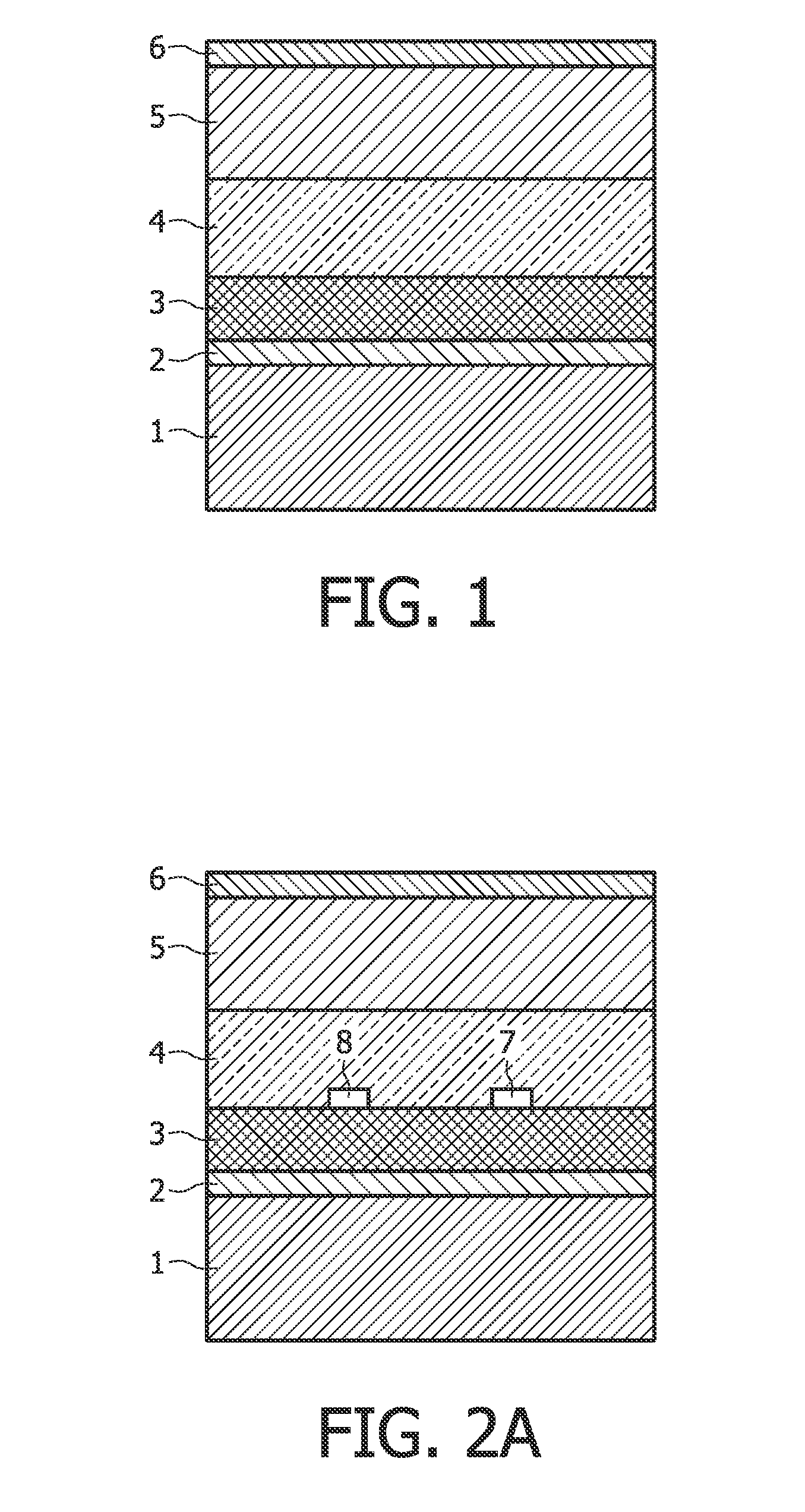
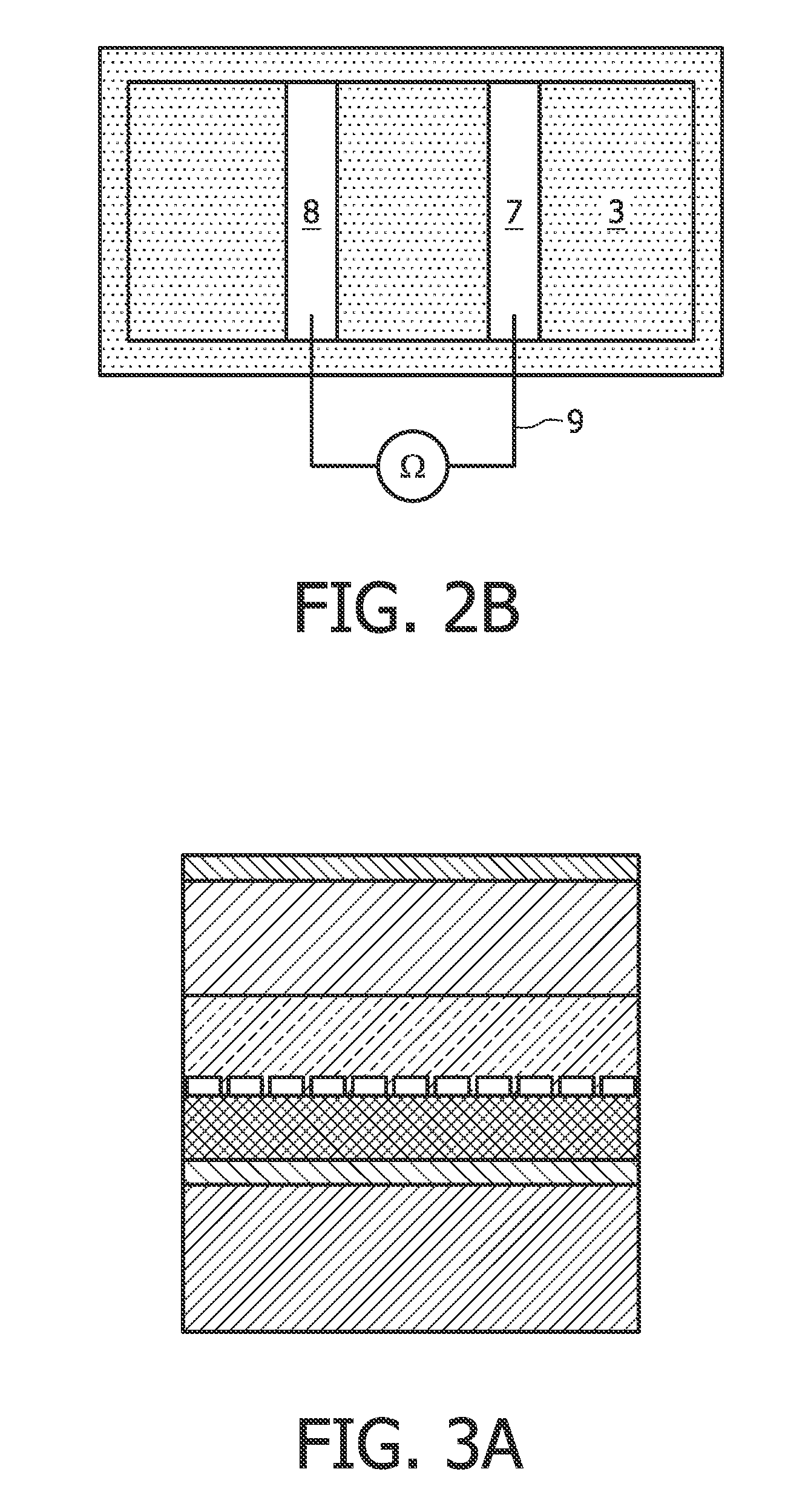
[0039]FIG. 1 shows a cross sectional view of the all solid-state thin film battery disclosed in WO-A-2005 / 027245. Using the deposition and integration technology described in this document, a stack can be manufactured that can be use to make an electrochemically tunable resistor. This stack comprises a substrate 1, onto which a current collector 2 has been deposited. An anode layer 3 has been deposited on the current collector layer 2 and on the anode layer 3 an electrolyte layer 4 has been deposited. On the electrolyte layer4 a cathode layer 5 and thereon a current collector layer 6 has been deposited. The stack structure thus obtained is described in WO-A-2005 / 027245.

[0040]In FIG. 1 the battery is depicted in the discharged state. In this situation the anode is completely de-lithiated (and the cathode fully lithiated). The resistance of the anode can be measured and will be roughly equal to the resistance of amorphous elemental silicon.

[0041]In its charged state the anode is fully...


PUM


Abstract

Presently, many variations of possible integrated resistors are utilized in IC design. However, depending on the electrical circuit it is often desirable that a resistor does not have a constant value, but rather that such a resistor has a variable controllable value. The invention relates to a solid-state variable resistor. The invention also relates to an electronic device, comprising such a solid-state variable resistor. The invention further relates to a method for producing a solid-state variable resistor.

Description

FIELD OF THE INVENTION[0001]The invention relates to a solid-state variable resistor. The invention also relates to an electronic device, comprising such a solid-state variable resistor. The invention further relates to a method for producing a solid-state variable resistor.BACKGROUND OF THE INVENTION[0002]Presently, many variations of possible integrated resistors are utilized in IC design. However, depending on the electrical circuit it is often desirable that a resistor does not have a constant value, but rather that such a resistor has a variable controllable value. Currently, MOSFETs can be used as tunable or variable resistors. In these devices the gate voltage can tune the resistance value across the semiconductor channel. In most MOSFETs it is hard to accurately tune the exact resistance of the semi-conductor channel. Very often only a low (“on” state) and a high (“off” state) resistance state are employed. This is directly related to the fact that below the threshold voltag...

Claims


Application Information

Patent Timeline
IPC IPC(8): H01M4/02H01L21/02H01M10/052H01M10/056H01M10/0562H01M10/0585H01M10/36
CPCH01C10/14H01M6/40H01M10/0436H01M10/052H01M10/056Y02E60/124H01M10/0585H01M10/347H01M2300/0068Y02E60/122H01M10/0562Y02E60/10Y02P70/50
Inventor NIESSEN, ROGIER ADRIANUS HENRICANOTTEN, PETRUS HENRICUS LAURENTIUSOP HET VELD, JOHANNES HUBERTUS GERARDUSPIJNENBURG, REMCO HENRICUS WILHELMUS
Owner KONINKLIJKE PHILIPS ELECTRONICS NV
Features
  • R&D
  • Intellectual Property
  • Life Sciences
  • Materials
  • Tech Scout
  • Unparalleled Data Quality
  • Higher Quality Content
  • 60% Fewer Hallucinations
Learn More