Led chip package structure using sedimentation and method for making the same

Inactive Publication Date: 2010-01-14
HARVATEK CORPORATION
View PDF3 Cites 16 Cited by
  • Summary
  • Abstract
  • Description
  • Claims
  • Application Information

AI Technical Summary

Benefits of technology

[0007]One particular aspect of the present invention is to provide an LED chip package structure using sedimentation and a method for making the same. Because the powder of the present invention can be fully deposited on the inner surface of the package body, “the condensing capability” and “the color and luster” of the present invention are goo

Problems solved by technology

However, the phosphor powder 40 does not be uniformly mixed into the colloid layer 4.
Hence, when the blue light generated by the blue LED can pass through the coll

Method used


Image

  • Led chip package structure using sedimentation and method for making the same
  • Led chip package structure using sedimentation and method for making the same
  • Led chip package structure using sedimentation and method for making the same

Examples


Example

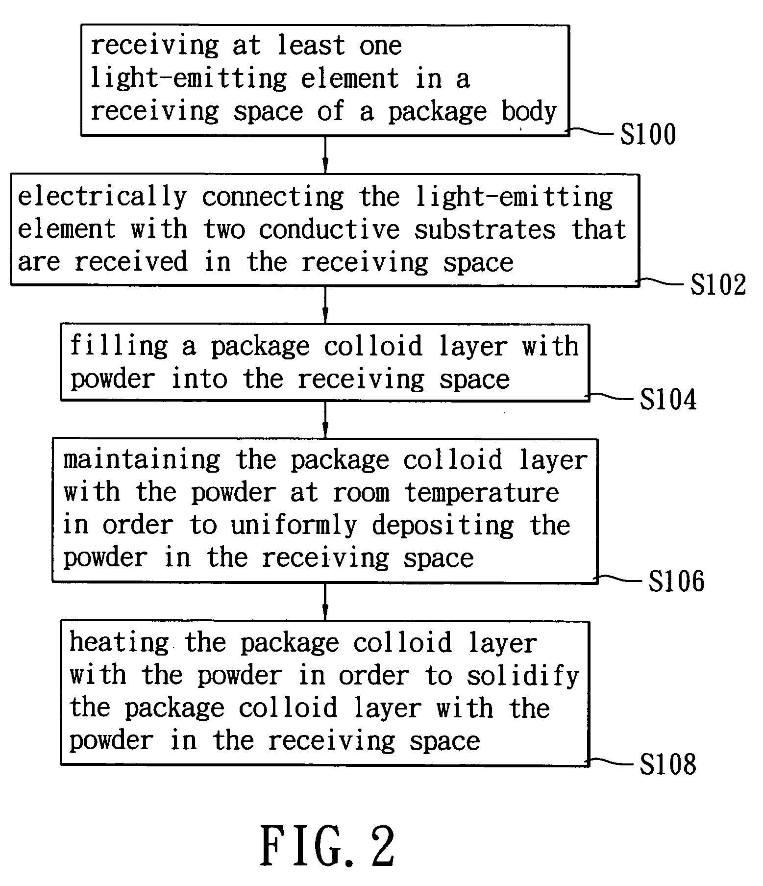
[0034]Referring to FIGS. 2 and 2A to 2C, the first embodiment of the present invention provides a method for making an LED chip package structure using sedimentation, including the following steps:

[0035]Step S100 is: referring to FIGS. 2 and 2A, receiving at least one light-emitting element la in a receiving space 20a of a package body 2a. In the first embodiment, the light-emitting element la can be a blue LED, and the package body 2a has a bowl shape. In addition, the light-emitting element 1a is firmly fixed on the inner surface of the bowl-shaped package body 2a via a chip-positioning layer 3a formed between the light-emitting element 1a and the package body 2a. Moreover, the chip-positioning layer 3a is solidified by curing to 155° C. during 3 hours in order to firmly fix the light-emitting element 1a on the inner surface of the bowl-shaped package body 2a.

[0036]Step S102 is: referring to FIGS. 2 and 2A, electrically connecting the light-emitting element 1a with two conductive...

Example

[0045]Moreover, after the step of S202, the second embodiment of the present invention further includes the following steps:

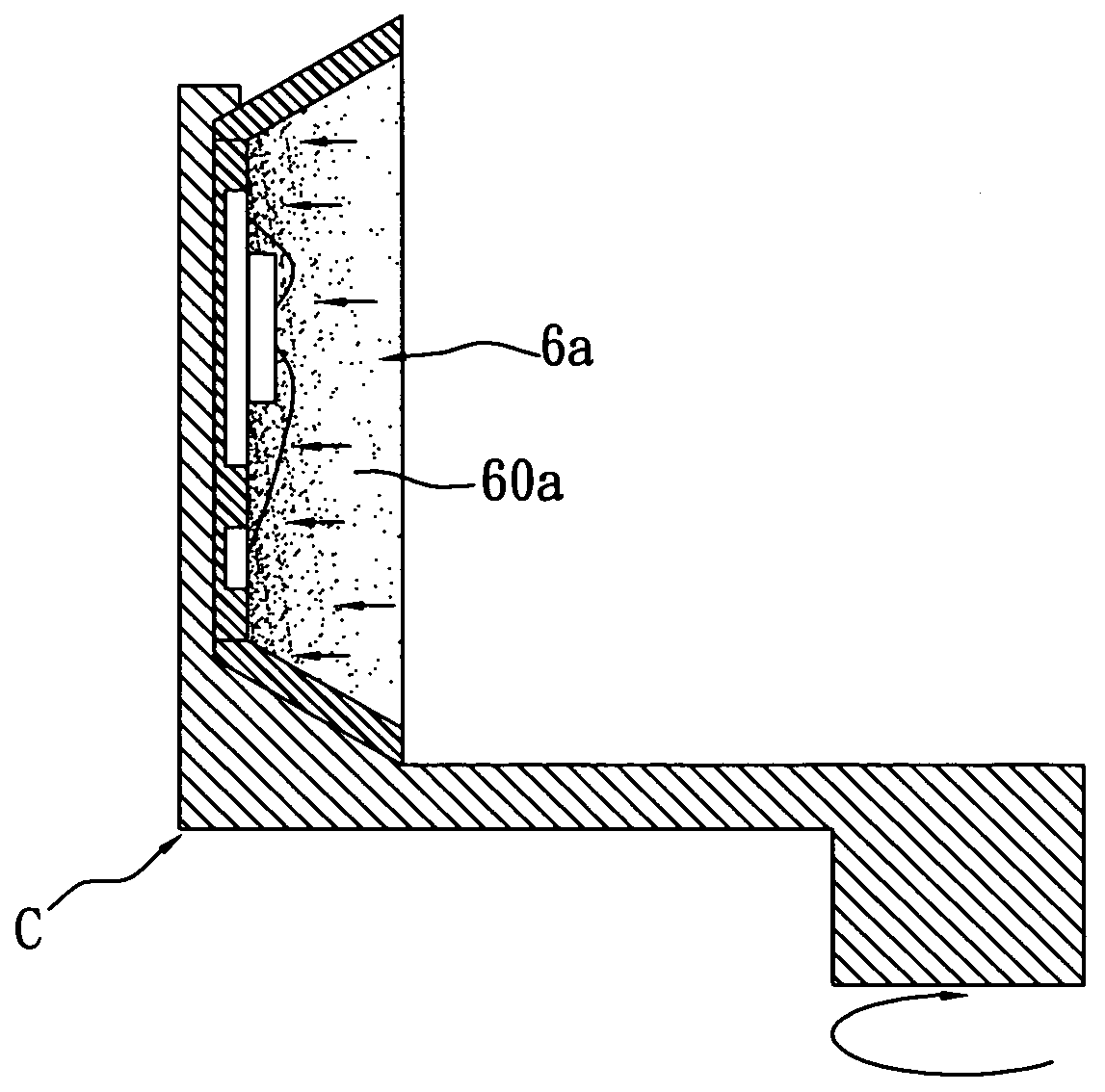
[0046]Step S204 is: referring to FIGS. 3 and 3A, filling a package colloid layer 6b with powder 60b into one part of a receiving space 20b of a package body 2b.

[0047]Step S206 is: referring to FIGS. 3 and 3B, maintaining the package colloid layer 6b with the powder 60b at room temperature in order to uniformly depositing the powder 60b′ in one part of the receiving space 20b. In other words, the powder 60b′ can be deposited on a light-emitting element 1b, two conductive substrates (40b, 41b) and an inner surface of the package body 2b. In addition, the room temperature is defined as 13-25° C., and the package colloid layer 6b is maintained at 1-168 hours according the properties of the package colloid layer 6b.

[0048]Step S208 is: heating the package colloid layer 6b′ with the powder 60b′ in order to solidify the package colloid layer 6b′ with the powder 60b′....

Example

[0053]Moreover, after the step of S302, the third embodiment of the present invention further includes the following steps:

[0054]Step S304 is: referring to FIGS. 4 and 4A, filling a transparent colloid layer 7c into one part of a receiving space 20c of a package body 2c in order to cover at least one light-emitting element 1c.

[0055]Step S306 is: heating the transparent colloid layer 7c to 80-150° C. during 1-6 hours in order to solidify the transparent colloid layer 7c.

[0056]Step S308 is: referring to FIGS. 4 and 4B, filling a package colloid layer 6c with powder 60c in the other part of the receiving space 20c of the package body 2c in order to form the package colloid layer 6c with the powder 60c on the transparent colloid layer 7c.

[0057]Step S310 is: referring to FIGS. 4 and 4C, maintaining the package colloid layer 6c with the powder 60c at room temperature in order to uniformly depositing the powder 60c′ on the transparent colloid layer 7c. In addition, the room temperature ...


PUM


Abstract

An LED chip package structure using sedimentation includes a package body, at least two conductive substrates, at least one light-emitting element, and a package unit. The package body has a receiving space. The two conductive substrates are received in the receiving space. The light-emitting element is received in the receiving space and electrically connected to the two conductive substrates. The package unit has a package colloid layer and a powder mixed into the package colloid layer, and the package unit is filled into the receiving space. The powder is uniformly deposited in the receiving space by maintaining the package unit at room temperature firstly and the powder is solidified in the receiving space by heating to a predetermined temperature.

Description

BACKGROUND OF THE INVENTION[0001]1. Field of the Invention[0002]The present invention relates to an LED chip package structure and a method for making the same, and particularly relates to an LED chip package structure using sedimentation and a method for making the same.[0003]2. Description of Related Art[0004]Referring to FIG. 1, a known LED package structure includes a substrate 1, an LED 2 disposed on the substrate 1, two wires 3, and a colloid layer 4 with phosphor powder 40.[0005]The LED 2 has a light-emitting surface 20 opposite to the substrate 1. The LED 2 has a positive electrode area 21 and a negative electrode area 22 electrically connected to two corresponding positive and negative electrode areas 11, 12 of the substrate 1 via the two 3 respectively. Moreover, the colloid layer 4 with the phosphor powder 40 covers the LED 2 and the two wires 3 for protecting the LED 2. Therefore, when the LED 2 is a blue LED, the blue light generated by the blue LED can pass through the...

Claims


Application Information

Patent Timeline
IPC IPC(8): H01L33/00H01L21/56
CPCH01L33/508H01L2933/0041H01L33/52H01L2924/181H01L2224/48091H01L2924/00014H01L2924/00012
Inventor WANG, BILYWU, SHIH-YUHUANG, CHAO-YUANYANG, PING-CHOUCHIANG, CHENG-YEN
Owner HARVATEK CORPORATION
Why Eureka
Try Eureka