Breakdown Voltages of Ultra-High Voltage Devices By Forming Tunnels

a technology of ultra-high voltage devices and tunnels, which is applied in the direction of semiconductor devices, transistors, electrical equipment, etc., can solve the problems of requiring the device to be replaced, the device is not efficient, and the on-resistance of high-voltage devices cannot be maintained. , to achieve the effect of increasing the breakdown voltage of the device and reducing the on-resistance of the high-voltage mos

a technology of ultra-high voltage devices and tunnels, which is applied in the direction of semiconductor devices, transistors, electrical equipment, etc., can solve the problems of requiring the device to be replaced, the device is not efficient, and the on-resistance of high-voltage devices cannot be maintained. , to achieve the effect of increasing the breakdown voltage of the device and reducing the on-resistance of the high-voltage mos

US20100006935A1Inactive Publication Date: 2010-01-14TAIWAN SEMICON MFG CO LTD

Image

  • Breakdown Voltages of Ultra-High Voltage Devices By Forming Tunnels
  • Breakdown Voltages of Ultra-High Voltage Devices By Forming Tunnels
  • Breakdown Voltages of Ultra-High Voltage Devices By Forming Tunnels

Examples


Embodiment Construction

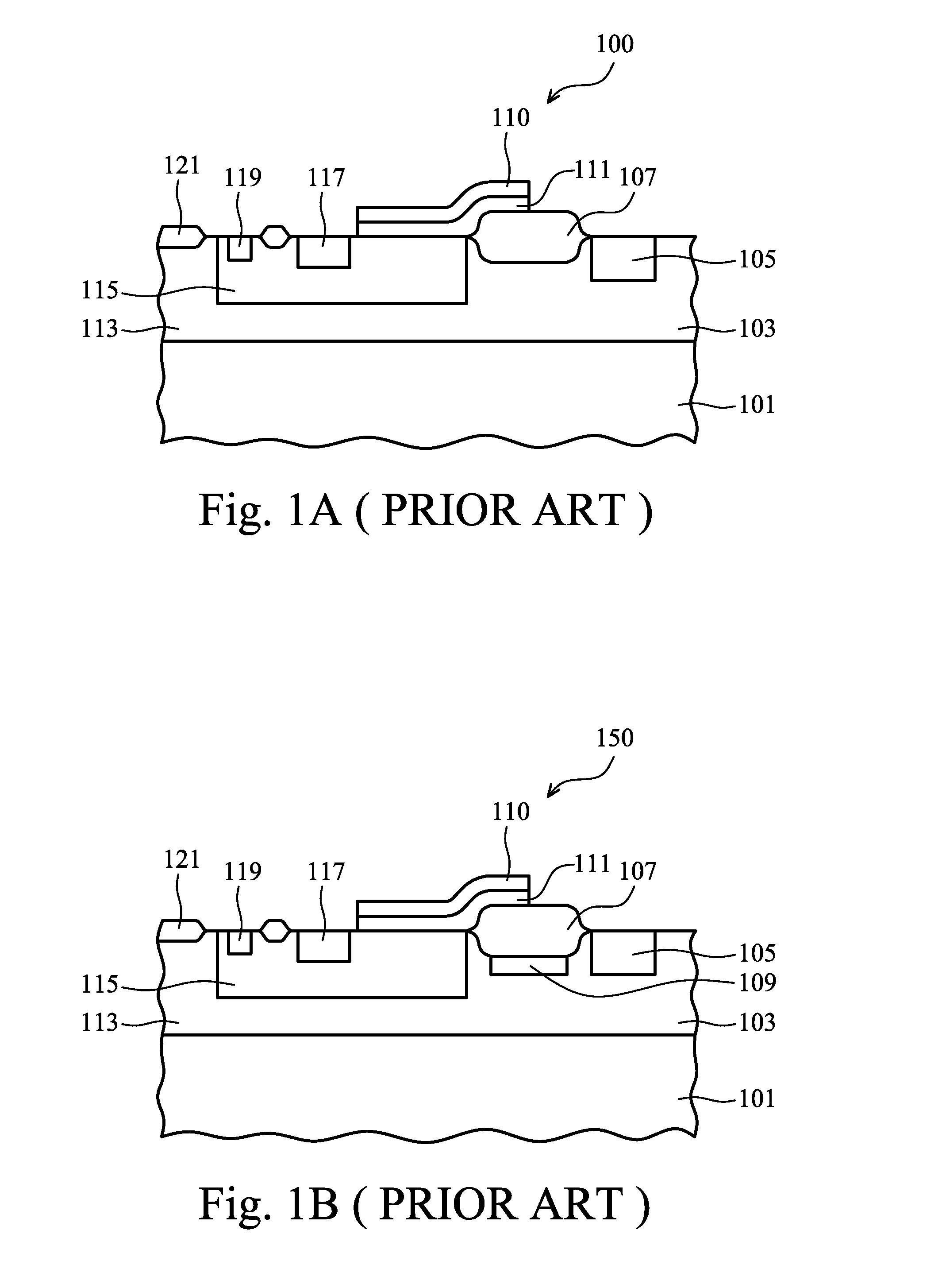
[0023]The making and using of the presently preferred embodiments are discussed in detail below. It should be appreciated, however, that the present invention provides many applicable inventive concepts that can be embodied in a wide variety of specific contexts. The specific embodiments discussed are merely illustrative of specific ways to make and use the invention, and do not limit the scope of the invention.

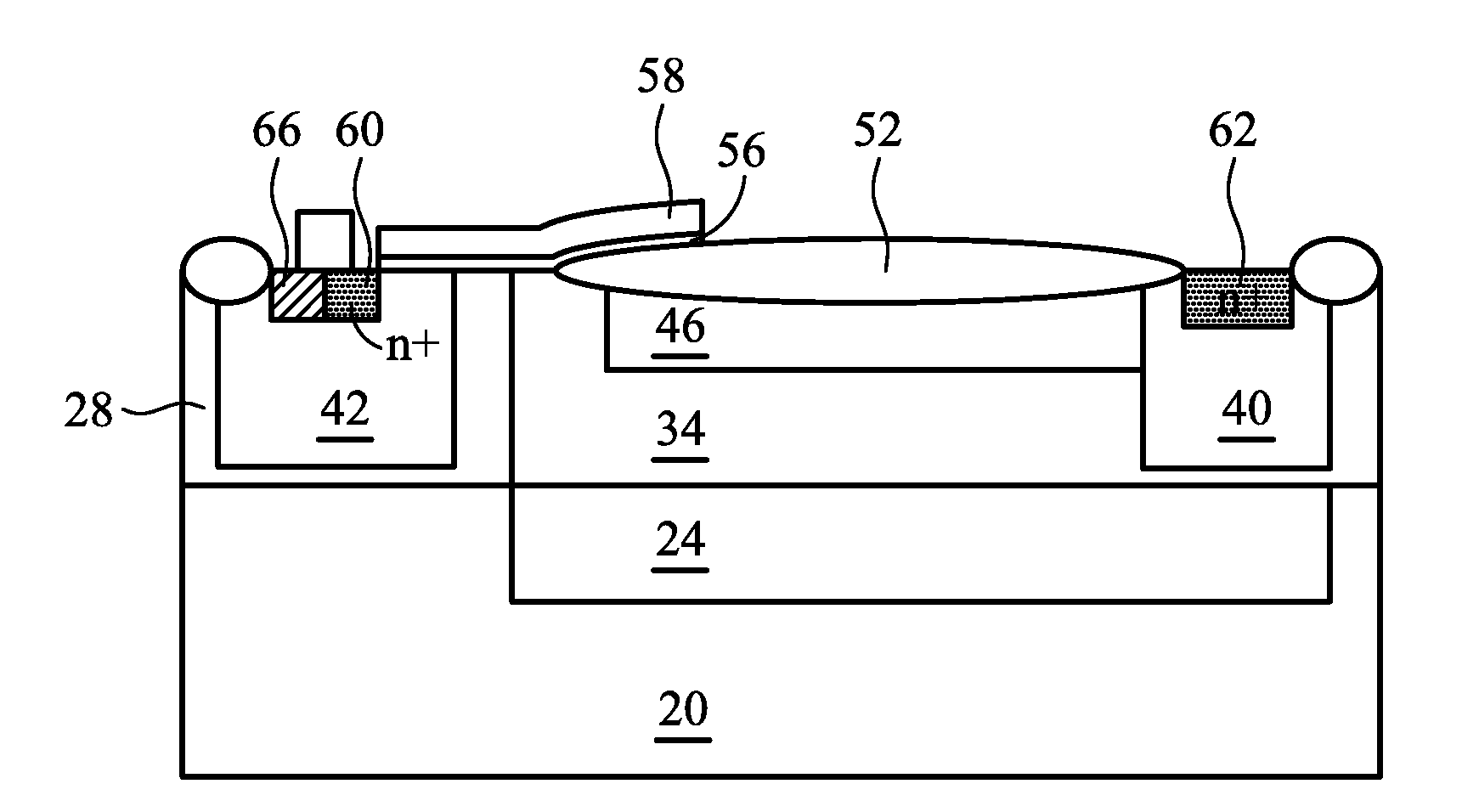
[0024]A novel high-voltage metal-oxide-semiconductor field-effect transistor (MOSFET) having a reduced on-resistance, an increased breakdown voltage, an increased stability, and the method of forming the same are provided. The manufacturing process of this device is detailed in the following paragraphs. Throughout the various views and illustrative embodiments of the present invention, like reference numbers are used to designate like elements.

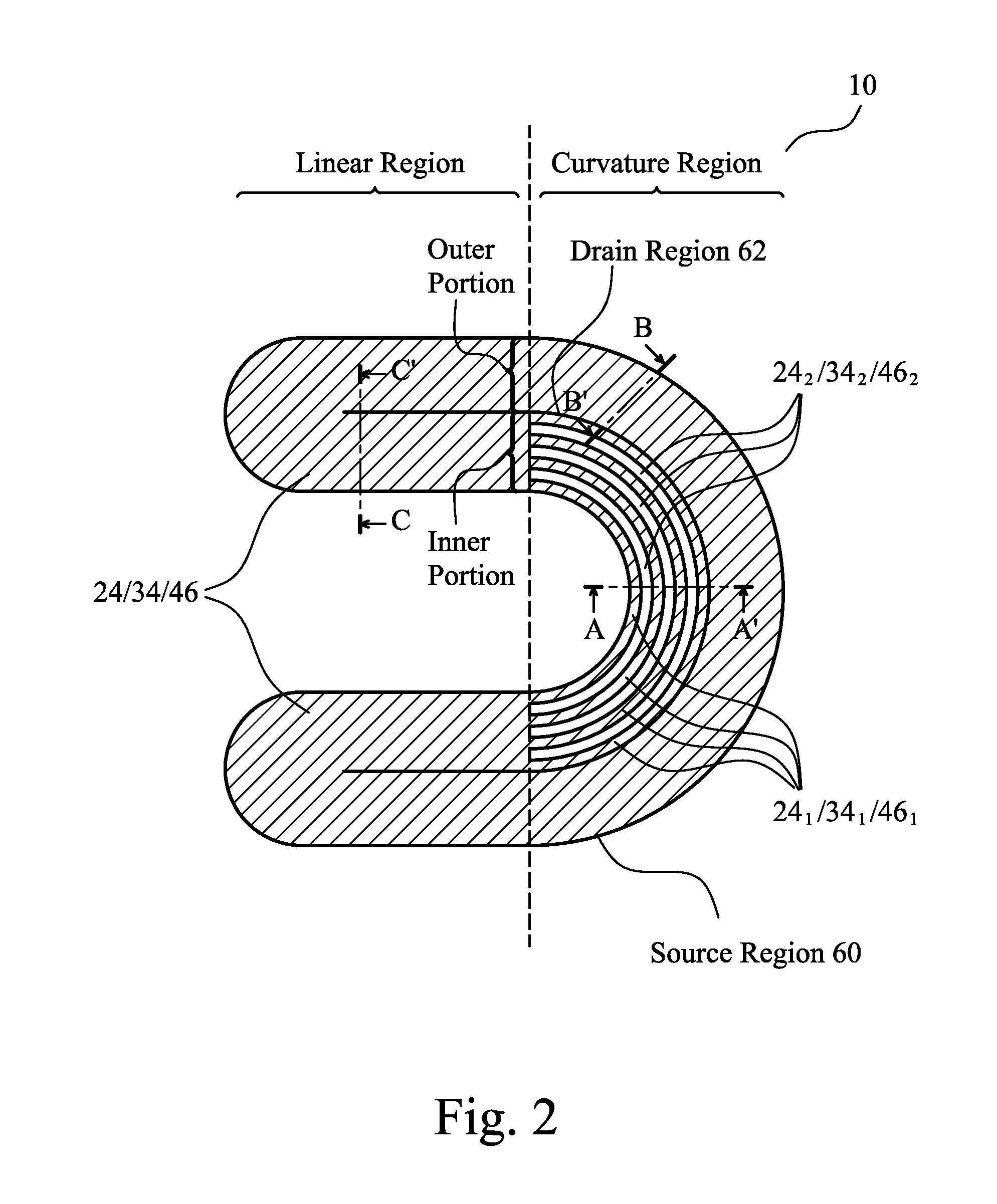
[0025]FIG. 2 illustrates a top view of UHV MOSFET 10. For a clearer view, only select components are illustrated. The remaining compon...


PUM


Abstract

A semiconductor structure includes a semiconductor substrate of a first conductivity type; a pre-high-voltage well (pre-HVW) in the semiconductor substrate, wherein the pre-HVW is of a second conductivity type opposite the first conductivity type; a high-voltage well (HVW) over the pre-HVW, wherein the HVW is of the second conductivity type; a field ring of the first conductivity type occupying a top portion of the HVW, wherein at least one of the pre-HVW, the HVW, and the field ring comprises at least two tunnels; an insulation region over the field ring and a portion of the HVW; a drain region in the HVW and adjacent the insulation region; a gate electrode over a portion the insulation region; and a source region on an opposite side of the gate electrode than the drain region.

Description

CROSS-REFERENCE TO RELATED APPLICATION[0001]The present application is related to commonly-assigned U.S. patent application Ser. No. 11 / 581,178, filed on Oct. 13, 2006, and entitled “Lateral Power MOSFET with High Breakdown Voltage and Low On-Resistance,” which application is hereby incorporated herein by reference.TECHNICAL FIELD[0002]This invention relates generally to semiconductor structures and methods, and more particularly to high voltage metal-oxide-semiconductor field-effect transistors (MOSFET).BACKGROUND[0003]Ultra-high voltage metal-oxide-semiconductor field effect transistors (MOSFET) were typically fabricated with coplanar drain and source regions. FIG. 1A shows an ultra-high voltage MOSFET device 100 in the prior art. Device 100 is formed on a p-type substrate 101, and another p-layer 113 is epitaxially grown on substrate 101. High-voltage p-well 115 is adjacent high-voltage n-well 103 in the epitaxially grown p-layer 113. N+ source 117 is positioned in the high-volta...

Claims


Application Information

Patent Timeline
14 Jan 2010
Publication
US20100006935A1
IPC
H01L29/78
CPC
H01L21/266; H01L29/0634; H01L29/0692; H01L29/7835; H01L29/42368; H01L29/66659; H01L29/0847
Inventors
HUANG, ERIC; HUANG, TSUNG-YI