Planar srfet using no additional masks and layout method
Active Publication Date: 2016-02-18
ALPHA & OMEGA SEMICON INC
View PDF7 Cites 2 Cited by
Summary
Abstract
Description
Claims
Application Information
AI Technical Summary
This helps you quickly interpret patents by identifying the three key elements:
Problems solved by technology
Method used
Benefits of technology
[0012]Another aspect of this invention is to provide new layout configurations of the MOSFET device integrated with Schottky diodes with the FET and Schottky regions arranged in optimized layout configurations such that higher cell density and improved device performances are achieved.
[0013]Another aspect of this invention is to provide semiconductor power device integrated with Schottky diode to increase the breakdown voltage of the device. Specifically, an aspect of this invention is to resolve the breakdown vulnerability at the bottom corners of the P+ pocket regions without changing the layout of the MOSFET devices that integrated with the Schottky diode for performance improvements.
[0014]Another aspect of this invention is to form the Junction Barrier controlled Schottky (JBS) rectifiers in the Schottky area with improved doping profile to increase the breakdown voltage without affecting the MOSFET cell performance. Furthermore, the JBS rectifiers are implemented with stripe, square closed cells, circular closed cells and hexagonal closed cells configurations.
[0015]Another aspect of this invention is to form the JBS rectifiers in the Schottky area with maximized Schottky area by forming the gate fingers as a comb shape with a bottom peripheral gate runner and not running the peripheral gate bus all the way around the die.
[0016]Briefly in a preferred embodiment this invention discloses a semiconductor power device supported on a semiconductor substrate of a first conductivity type having a bottom layer functioning as a bottom electrode and an epitaxial layer overlying the bottom layer having a same conductivity type as the bottom layer. The semi
Problems solved by technology
However, conventional ways of manufacturing the planar MOSFET devices with integrated Schottky diodes often require additional masks for the formation of the Schottky diodes in Schottky regions between the MOSFET cells.
Therefore, higher manufacturing costs and more complicate processes are necessary for implementing the planar MOSFET device with the Schottky diodes.
However, there is a tradeoff that due to an increase of the series resistance.
However, these devices still have the limitatio
Method used
Image
Click on the blue label to locate the original text in one second.
Reading with bidirectional positioning of images and text.
Examples
Example
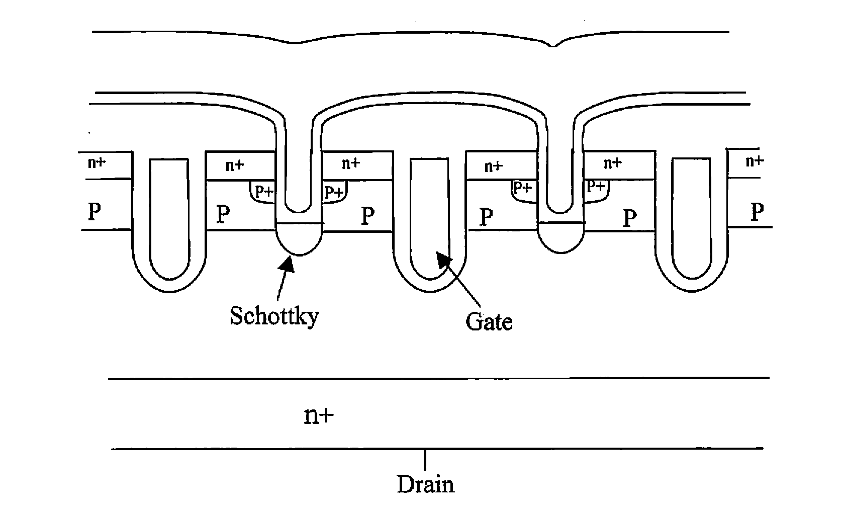
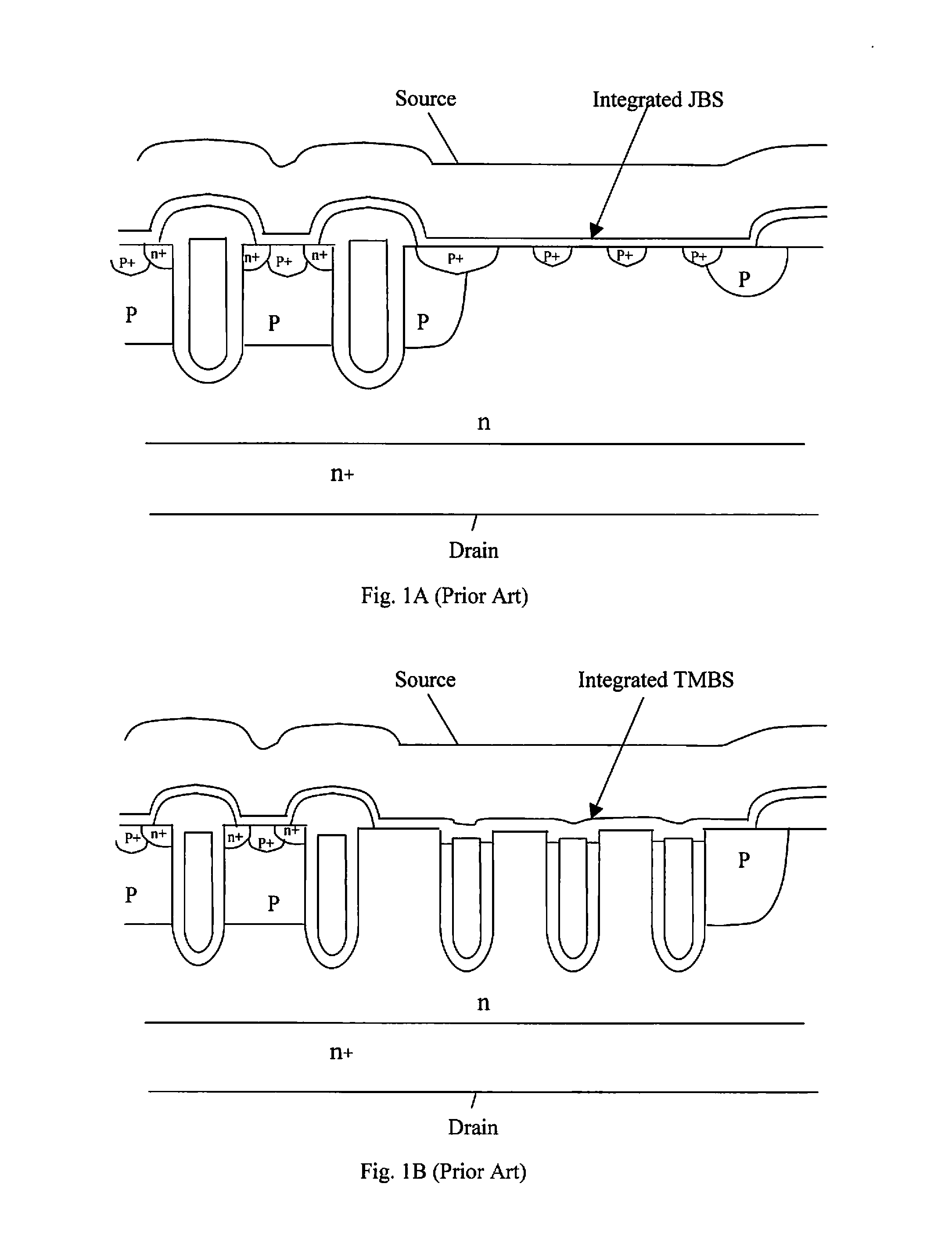
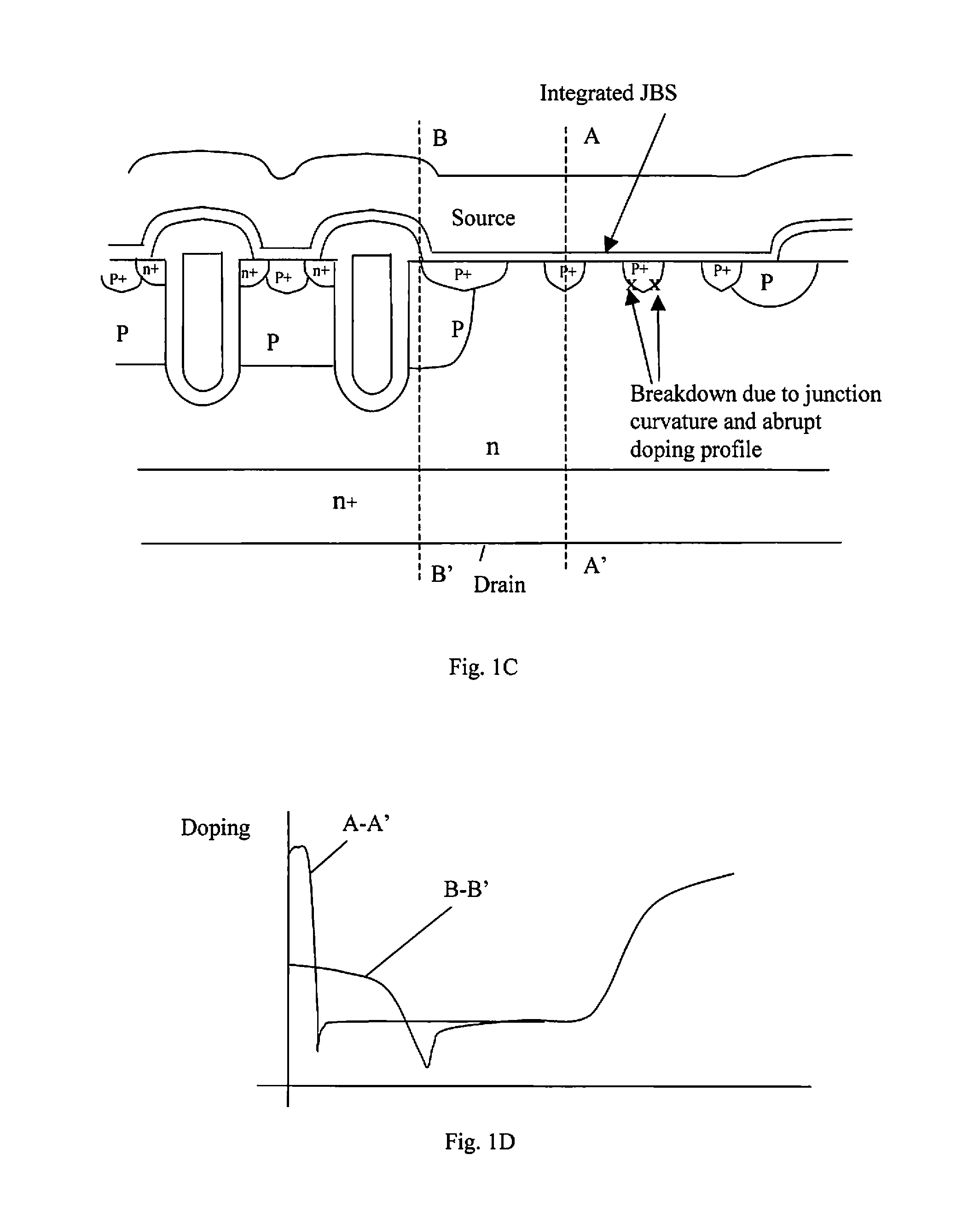
[0039]Referring to FIGS. 3A and 3B for the side cross sectional views of the JBS area to provide the rectification function for a MOSFET device. FIG. 3A shows a blank implant of a low dose of body type dopant ions. For N channel MOSFET device, Boron ions with dosage 5×10¹¹ to 5×10¹² / cm2 may be implanted into the epitaxial layer with energy from 40-500 Kev, preferably with 80-300 Kev. The blank implant of the body type dopant ions is to compensate and lower the doping concentration of a portion of the epitaxial layer to increase epitaxial layer breakdown voltage. In FIG. 3B, the body dopant is then diffused by applying an elevated diffusion temperature ranging from 1000 to 1150 degrees for 1 to 3 hours to diffusion the body type dopant into a depth shallower than the depth of MOSFET body region form in a later step. The implanting body type dopant ions compensate a portion of epitaxial dopant and generate an N− region in the epitaxial layer. This would not significantly affect the MO...
PUM
Abstract
A semiconductor power device is supported on a semiconductor substrate of a first conductivity type with a bottom layer functioning as a bottom electrode and an epitaxial layer overlying the bottom layer with a same conductivity type as the bottom layer. The semiconductor power device includes a plurality of FET cells and each cell further includes a body region of a second conductivity type extending from a top surface into the epitaxial layer. The body region encompasses a heavy body dopant region of second conductivity type. An insulated gate is disposed on the top surface of the epitaxial layer, overlapping a first portion of the body region. A barrier control layer is disposed on the top surface of the epitaxial layer next to the body region away from the insulated gate. A conductive layer overlies the top surface of the epitaxial layer covering a second portion of the body region and the heavy body dopant region extending over the barrier control layer forming a Schottky junction diode.
Description
[0001]This patent application is a Continuation application of a co-pending application Ser. No. 13 / 362,604 filed Jan. 31, 2012, and application Ser. No. 13 / 362,604 is a Divisional application and claims the Priority Date of another application Ser. No. 11 / 906,476 filed by common inventors of this application on Oct. 1, 2007 now issued as U.S. Pat. No. 8,110,869. application Ser. No. 11 / 906,476 is a Continuation in Part (CIP) application of two co-pending applications with Ser. Nos. 11 / 056,346 and 11 / 413,249 filed by a common Inventor of this application on Feb. 11, 2005 and Apr. 29, 2006 and now issued into U.S. Pat. Nos. 7,285,822 and 7,436,022 respectively. The Disclosures made in these application Ser. Nos. 11 / 056,346, 11 / 413,249, 11 / 906,476 and 13 / 362,604, are hereby incorporated by reference.BACKGROUND OF THE INVENTION[0002]1. Field of the Invention[0003]The invention relates generally to the semiconductor power devices. More particularly, this invention relates to an improved...
Claims
Application Information
Patent Timeline
Application Date:The date an application was filed.
Publication Date:The date a patent or application was officially published.
First Publication Date:The earliest publication date of a patent with the same application number.
Issue Date:Publication date of the patent grant document.
PCT Entry Date:The Entry date of PCT National Phase.
Estimated Expiry Date:The statutory expiry date of a patent right according to the Patent Law, and it is the longest term of protection that the patent right can achieve without the termination of the patent right due to other reasons(Term extension factor has been taken into account ).
Invalid Date:Actual expiry date is based on effective date or publication date of legal transaction data of invalid patent.