Method for manufacturing an edge termination for a silicon carbide power semiconductor device

a technology of silicon carbide power semiconductor and edge termination, which is applied in the direction of semiconductor devices, diodes, electrical apparatus, etc., can solve the problems of increasing alignment precision and reproducibility, reducing production yield, and manufacturing costs, so as to improve the breakdown properties of the device, reduce the cost of manufacturing, and prevent or at least reduce the effect of electric field peak

Active Publication Date: 2018-10-30
HITACHI ENERGY LTD
View PDF12 Cites 1 Cited by
  • Summary
  • Abstract
  • Description
  • Claims
  • Application Information

AI Technical Summary

Benefits of technology

[0006]It is an object of the invention to provide a method for manufacturing an edge termination for a power silicon carbide semiconductor device which is easy to manufacture and efficiently prevents or at least lowers any electric field peaks in the termination region, thereby improving the breakdown properties of the device.
[0008]Due to the lowering of the doping concentration of the drift layer in the (n−−) doping reduction layer, the electric field peaks can be lowered in the edge region and thus, also the electric field distribution towards the edge of the device may be smoothed. Due to the low doping concentration in the doping reduction layer, no high electric fields extend to the surface of the device in the termination (edge) region. By such doping reduction layers the breakdown voltage of the device may be increased and the reverse current resulting from impact ionization at junction termination is lowered. A lower leakage current again, enables the device to be operated with enhanced blocking stability. The doping reduction layer can be implemented in combination with known termination means for lowering the electric field in the edge region such as p doped guard rings, junction termination extensions or floating metal rings (also called field plates), not excluding other known means.
[0009]The implantation of light ions (helium or hydrogen (protons)) to compensate the original concentration of the drift layer by introduced radiation point defects, thereby creating a doping reduction layer, may be restricted to the edge region. This results in a device, in which the termination region has a higher breakdown voltage than the active bulk region, so that the device blocking stability may be enhanced in the inventive device. In case of biasing the device above the breakdown voltage, the lower breakdown voltage in the bulk functions like a protection of the edge termination, which prevents the wear-out of junction termination surface passivation (the most sensitive part of device from reliability viewpoint) and increases reliability.
[0010]Helium or hydrogen (protons) is applied as a first ion to compensate the original doping concentration of the drift layer. Such light ions can be introduced into higher depths than heavier ions at the same implant energy. Both ions have the advantage that they are stopped in silicon carbide in a small depth range of less than 1 μm so that locally limited layers (in depth direction) may be created. Thereby, it is possible to protect the places of highest electric fields particularly.
[0012]Depending on the application, a single or multiple ion peaks with different energies can further enhance the breakdown voltage without increasing the leakage current.

Problems solved by technology

This makes the manufacturing costly.
At the same time, it increases demands on the alignment precision and reproducibility of lithographical processing steps and / or it reduces production yield.
Due to the misalignment of highly and lightly doped p-regions in production, the enhancement of the blocking voltage might not be as high as predicted by the device simulation.

Method used


Image

  • Method for manufacturing an edge termination for a silicon carbide power semiconductor device
  • Method for manufacturing an edge termination for a silicon carbide power semiconductor device
  • Method for manufacturing an edge termination for a silicon carbide power semiconductor device

Examples


Embodiment Construction

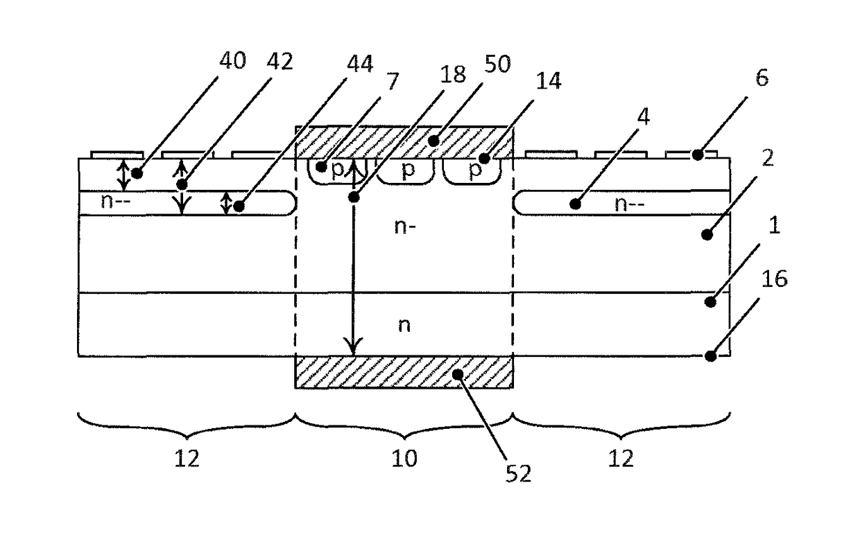
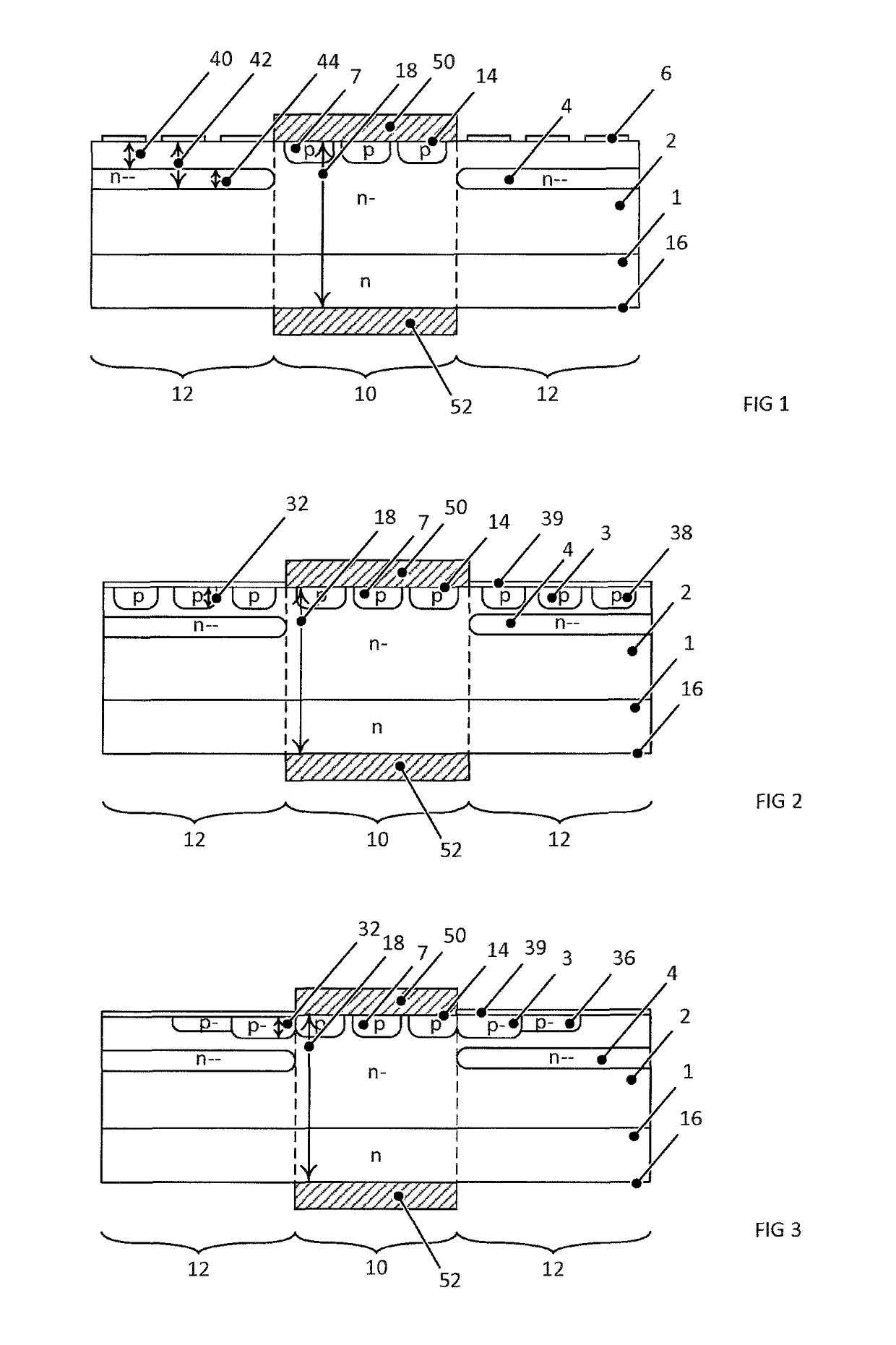
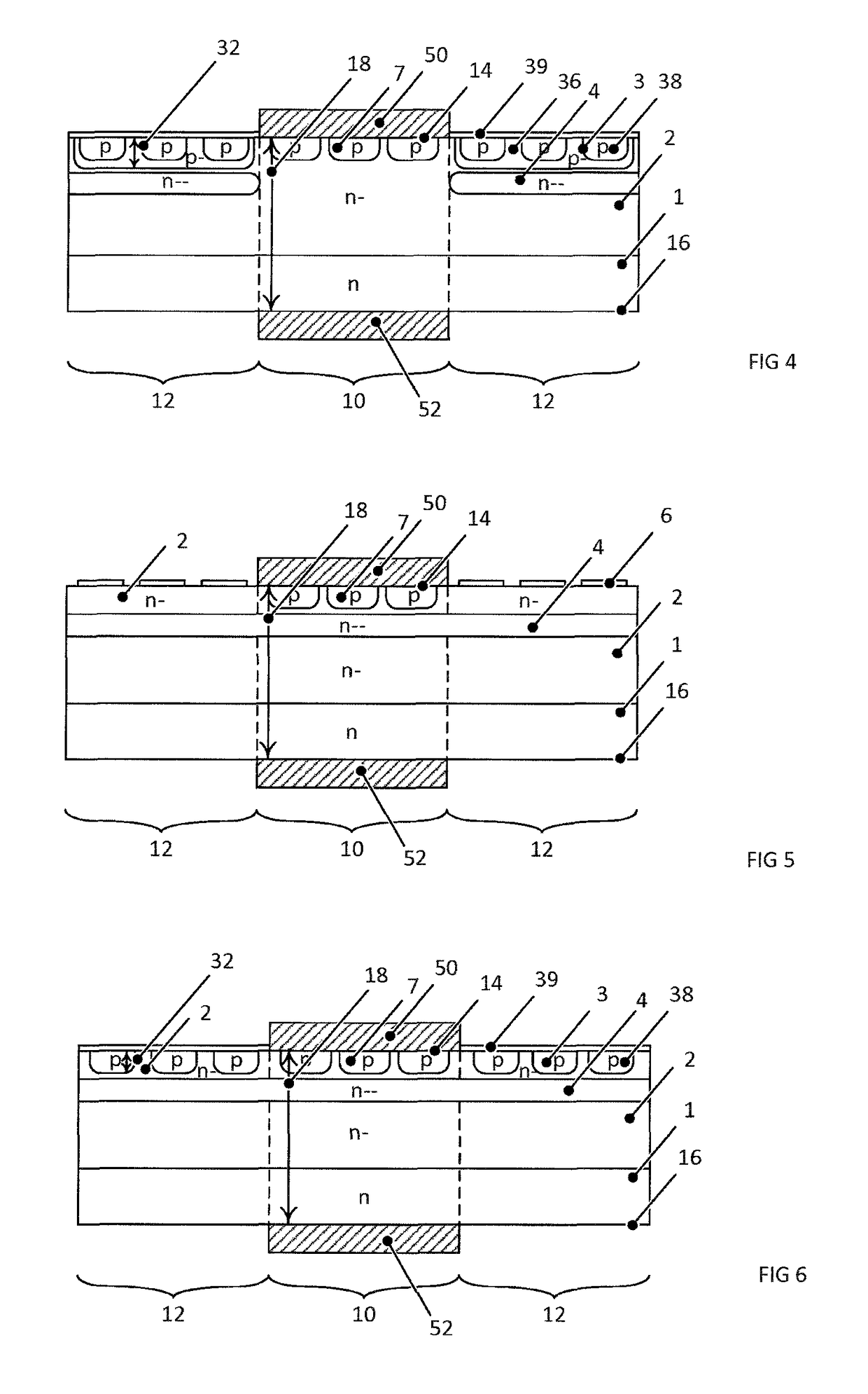
[0027]FIGS. 1 to 8 and 16 show an inventive silicon carbide power semiconductor device in form of a Junction Barrier Schottky (JBS) diode or a merged PiN Schottky (MPS) diode having a central region 10 and an edge region 12 (termination region) between a first main side 14 and a second main side 16 opposite to the first main side 14. An n doped silicon carbide substrate layer 1 is arranged on the second main side 16. An n− doped silicon carbide drift layer 2 which is lower doped than the n doped SiC substrate 1, is arranged on the first main side 14.

[0028]In the edge region 10 an (n−−) doped doping reduction layer 4 is arranged, which has a lower doping concentration than the drift layer 2, wherein the doping reduction layer 4 is arranged in a layer depth range 44 between a doping concentration minimum 40 below the first main side 14 up to a maximum doping reduction layer depth 42. This maximum depth 42 is lower than the thickness of the power semiconductor device. The doping concen...


PUM

PropertyMeasurementUnit
depthaaaaaaaaaa
depthaaaaaaaaaa
energyaaaaaaaaaa

Abstract

A method for manufacturing an edge termination structure for a silicon carbide power semiconductor device having a central region and an edge region is provided. The following manufacturing steps are performed: a) providing an n-doped silicon carbide substrate, b) epitaxially growing a silicon carbide n-doped drift layer on the substrate, which has a lower doping concentration than the substrate, c) creating at least one p-doped termination layer by implanting a second ion up to a maximum termination layer depth and annealing on the first main side, d) forming a doping reduction layer having a depth range, which doping reduction layer comprises at least one doping reduction region, wherein a depth of a doping concentration minimum of the doping reduction layer is greater than the maximum termination layer depth, wherein for the creation of each doping reduction region: implanting a first ion with an implantation energy in the drift layer at least in the edge region, wherein the first ion and the at least one implantation energy are chosen such that the doping reduction layer depth range is less than 10 μm, e) annealing the doping reduction layer, wherein step d) and e) are performed such that the doping concentration of the drift layer is reduced in the doping reduction layer.

Description

TECHNICAL FIELD[0001]The invention relates to the field of power electronics and more particularly to a method for manufacturing an edge termination structure for a silicon carbide power semiconductor device, to a method to manufacture a silicon carbide power semiconductor device having such an edge termination structure and to a silicon carbide power semiconductor device as such.BACKGROUND ART[0002]A conventional silicon carbide (SiC) Schottky diode comprises an n-type SiC substrate, on which an n− doped drift layer is epitaxially grown. This drift layer is contacted by a Schottky contact. Surrounding the Schottky contact a p doped junction termination extension (JTE) layer may be arranged in order to lower the electric field peak on the edge of the Schottky contact and to smoothly lower the electric field towards the edge of the diode. Additionally to the JTE layer, concentric floating p doped guard rings may be around the JTE layer to avoid high field peaks on the surface of the ...

Claims


Application Information

Patent Timeline
Patent Type & Authority Patents(United States)
IPC IPC(8): H01L29/87H01L29/16H01L29/872H01L29/66H01L29/06H01L29/739H01L29/868
CPCH01L29/872H01L29/0619H01L29/6606H01L29/7395H01L29/1608H01L29/868H01L29/0615H01L29/32H01L29/36H01L29/8083
Inventor VOBECKY, JAN
Owner HITACHI ENERGY LTD
Why Eureka
Try Eureka