SOI semiconductor device

a semiconductor device and semiconductor technology, applied in the field of insulated gate field effect transistors and bipolar transistors, can solve the problems of increasing the manufacturing process of the device, the trenching required for isolation of the device-forming region, and the inability to complete the final stage of the device, so as to improve the breakdown voltage and improve the breakdown voltage. , the effect of improving the breakdown voltag

Inactive Publication Date: 2005-04-26
HITACHI LTD
View PDF13 Cites 2 Cited by
  • Summary
  • Abstract
  • Description
  • Claims
  • Application Information

AI Technical Summary

Benefits of technology

[0019]However, when a voltage close to the breakdown voltage is applied to the N-type MOS field-effect transistor illustrated in FIG. 2A, the N-type layer excluding the p-body layer becomes fully depleted, so that it can be regarded as a single capacitor. Its capacitance is denoted Csi. The buried insulating film, for which a silicon oxide film is employed in many cases, has also a capacitance as a matter of course. This capacitance is denoted Cox. Then, when the voltage close to the breakdown voltage is applied, the SIO substrate can be modeled as a series connection of the capacitors of Csi and Cox. Usually, a support substrate under the buried oxide film also has a capacitance. However, in a computer simulation employed for the present invention, the support substrate is regarded as a complete conductor, and approximations are made on the basis of this assumption. Further, modeling is performed such that the potential of the interface of the support substrate contacting the buried oxide film is set to the ground potential. Thus, the capacitance of the support substrate is ignored in this modeling process as well. When a voltage V is applied to the drain electrode, the applied voltage V is divided between the silicon substrate and the buried oxide film according to the ratio between the capacitance Csi and the capacitance Cox. The voltage applied to the buried oxide film when the voltage V is applied to the drain electrode can be expressed as (Csi×V) / (Csi+Cox). The larger Csi becomes, the larger the voltage applied to the buried oxide film can be made. Consequently, the voltage applied to the silicon substrate is accordingly reduced. The breakdown voltage of the device is thus improved. Setting the Csi to be large or setting the concentration of the substrate to be high can increase the voltage applied to the buried oxide film. The breakdown voltage of the device is thereby improved.
[0031]According to the present invention, an increased breakdown voltage N-channel MOS field-effect transistor, an increased breakdown voltage P-channel MOS field-effect transistor, an increased breakdown voltage NPN transistor, and an increased breakdown voltage PNP transistor can be obtained without increasing the thickness of a silicon layer and the thickness of a buried oxide film.

Problems solved by technology

However, when the buried insulating film becomes thick, a warp in a wafer increases in the manufacturing process of the device.
Consequently, the process at the final stage in completion of the device cannot be performed.
However, if the thickness of the silicon layer is increased, it takes much time to form trenches required for isolation of a device-forming region.
For this reason, throughput is reduced, so that a cost problem arises.
In addition, it becomes difficult to form a completely vertical deep trench and cover the trench with an insulated film tightly.
Accordingly, if the high concentration N-type layer is present in the silicon layer with its thickness reduced, a high breakdown voltage cannot be obtained.
When the concentration of the substrate becomes high, even if the drain-source distance is increased, the depletion layer formed between the p-body layer and the N-type substrate cannot extend sufficiently large.
Thus, it becomes impossible to achieve the breakdown voltage of 300 V. For this reason, if the N-channel MOS field-effect transistor with the breakdown voltage of 300 V is desired, there is no way other than increasing the thickness of the silicon layer or the thickness of the buried oxide film.
However, in the case of an 8-inch SOI substrate, for example, when the thickness of the buried oxide film exceeds 3.0 μm, a warp in the wafer increases during the manufacturing process of the device, so that manufacture of the device cannot be completed.
On the other hand, when the thickness of the silicon layer becomes thick, it takes additional time to form the trenches for device isolation.
Thus, throughput is reduced, and it also becomes difficult to form a vertical deep trench and cover the trench with an insulating film tightly.

Method used


Image

  • SOI semiconductor device
  • SOI semiconductor device
  • SOI semiconductor device

Examples


first embodiment

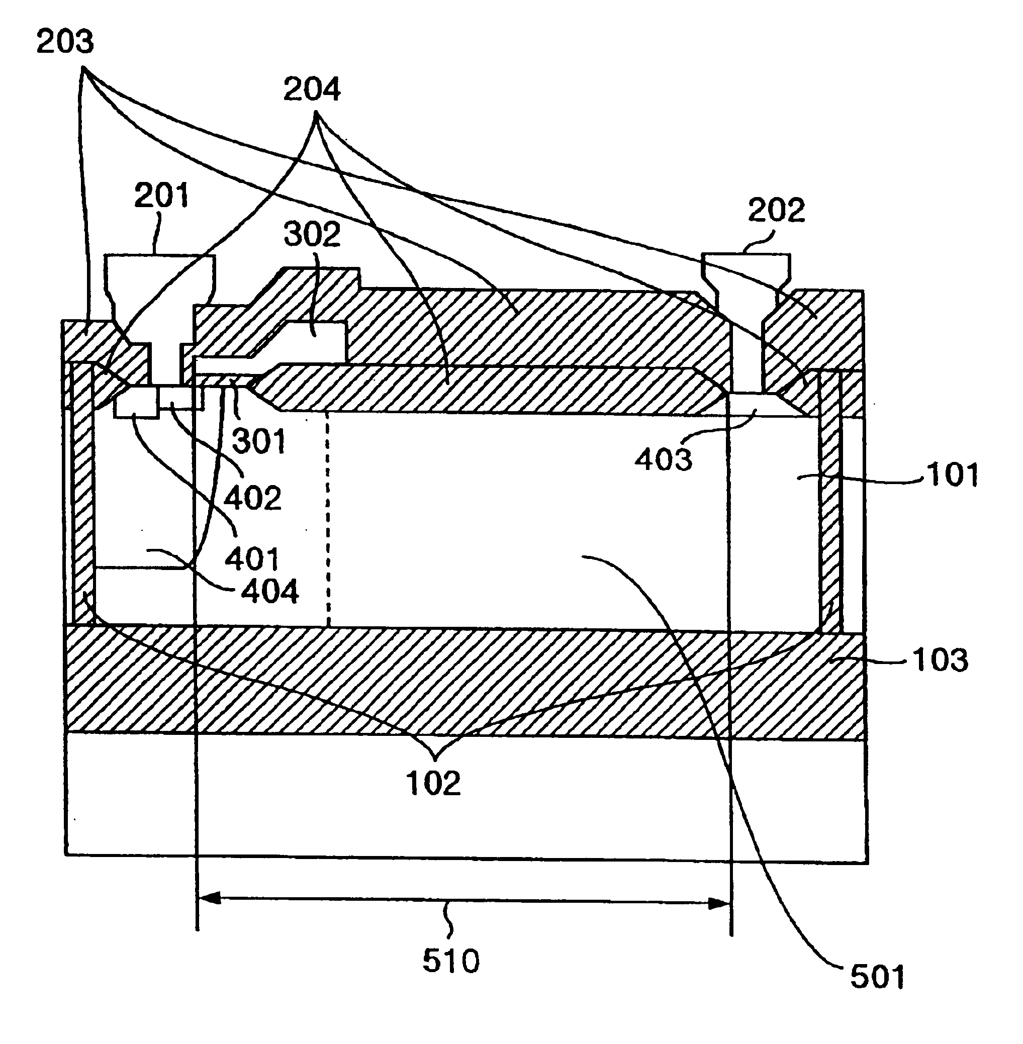
[0051]First, FIG. 1 shows a semiconductor device according to the present invention, and is a vertical sectional view illustrating the structure of an N-channel MOS field-effect transistor. The N-channel MOS field-effect transistor comprises the source electrode 201, and the drain electrode 202 and gate electrode 302 disposed in a lateral direction via the field oxide film 204, on the SOI substrate 101 having the N-type device-forming region. The transistor further comprises the gate oxide film 301, high concentration P-type layer 401, high concentration N-type layer 402, high concentration N-type layer 403, and p-type layer or p-body layer 404. The gate oxide film 301 is in contact with the gate electrode 302. The high concentration P-type layer 401 is in contact with the source electrode 201, and the high concentration N-type layer 402 is in contact with the source electrode 201 and the gate oxide film 301. The high concentration N-type layer 403 is in contact with the drain elect...

second embodiment

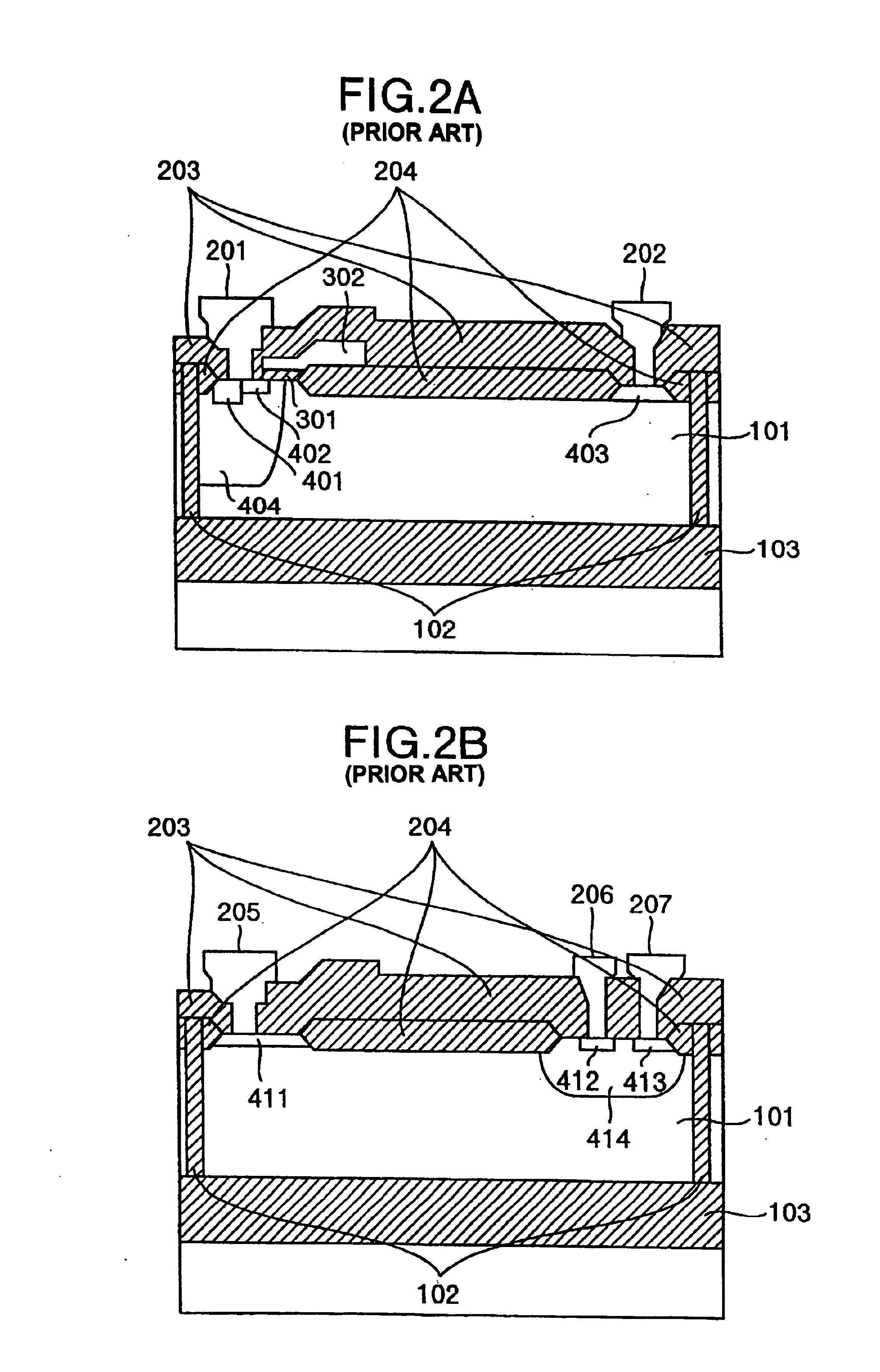
[0053]FIG. 4 shows a semiconductor device according to the present invention, and is a vertical sectional view illustrating the structure of an NPN bipolar transistor. The NPN bipolar transistor comprises the collector electrode 205, and the base electrode 206 and the emitter electrode 207 disposed in the lateral direction via the field oxide film 204, on the SOI substrate 101 having the N-type device-forming region. The transistor further comprises the high concentration N-type layer 411, high concentration P-type layer 412, high concentration N-type layer 413, and p-type base layer 414. The high concentration N-type layer 411 is in contact with the collector electrode 205. The high concentration P-type layer 412 is in contact with the base electrode 206. The high concentration N-type layer 413 is in contact with the emitter electrode 207. The P-type base layer 414 is in contact with the high concentration p-type layer 412 and the high concentration N-type layer 413. This transisto...

third embodiment

[0055]FIG. 5 shows a semiconductor device according to the present invention, and is a vertical sectional view illustrating an N-channel MOS field-effect transistor. The N-channel MOS field-effect transistor comprises the source electrode 201, and the drain electrode 202 and the gate electrode 302 disposed in the lateral direction via the field oxide film 204, on the SOI substrate having the N-type device-forming region. The transistor further comprises the gate oxide film 301 in contact with the gate electrode 302, high concentration P-type layer 401, high concentration N-type layer 402, high concentration N-type layer 403, and p-type layer or p-body layer 404. The high concentration P-type layer 401 is in contact with the source electrode 201. The high concentration N-type layer 402 is in contact with the source electrode 201 and the gate oxide film 301. The high concentration N-type layer 403 is in contact with the drain electrode 202. The p-body layer 404 is in contact with the ...


PUM


Abstract

A power IC for an automobile engine control unit incorporating at least one semiconductor device comprising an N-channel insulated-gate filed-effect transistor formed on an SOI substrate, having an N-type layer having a concentration higher than a concentration of an N-type layer in contact with a p-body layer contacting a gate oxide film of the transistor. The high concentration N-type layer is formed in a region covering at most 95% of the source-drain distance between the p-body layer and a drain electrode of the transistor in the silicon substrate over an interface of a buried oxide film, the silicon substrate being in contact with both the field oxide film and the high concentration N-type layer contacting the drain electrode.

Description

CROSS-REFERENCE TO RELATED APPLICATIONS[0001]This is a Divisional application of Ser. No. 10 / 393,951, filed Mar. 24, 2003, now U.S. Pat. No. 6,750,513, which is a Division of application Ser. No. 10 / 101,162, filed Mar. 20, 2002, now abandoned, the entire disclosure of which is hereby incorporated by reference.BACKGROUND OF THE INVENTION[0002]The present invention relates to a semiconductor device and a method of manufacturing the semiconductor device. More specifically, the invention relates to an insulated-gate field-effect transistor and a bipolar transistor, both formed on an SOI substrate.[0003]In a high breakdown voltage semiconductor device formed on the SOI (Silicon On Insulator) substrate, the magnitude of the breakdown voltage of the device determines the thickness of a silicon layer and the thickness of a buried insulating film. The silicon layer is the active region where the device is formed, and is formed over a support silicon substrate via the insulating film. The bre...

Claims


Application Information

Patent Timeline
Patent Type & Authority Patents(United States)
IPC IPC(8): H01L21/02H01L21/331H01L21/762H01L21/70H01L27/12H01L29/66H01L21/336H01L29/78H01L21/84H01L29/73H04M3/00G09G3/28H01L29/02H01L29/08H04M3/18H01L21/77H01L21/8222H01L21/8248H01L21/8249H01L27/06H01L27/08H01L29/10H01L29/786
CPCH01L21/76264H01L21/84H01L27/1203H01L29/66265H01L29/66674H01L29/7317H01L29/7824H04M3/005G09G3/28H01L21/76283H01L29/0847H04M2201/06H04M3/18H01L29/1083H01L29/66681
Inventor OHYANAGI, TAKASUMIWATANABE, ATSUO
Owner HITACHI LTD
Why Eureka
Try Eureka