Mold for pattern transfer

Inactive Publication Date: 2010-01-14
PIONEER CORP
View PDF3 Cites 2 Cited by
  • Summary
  • Abstract
  • Description
  • Claims
  • Application Information

AI Technical Summary

Benefits of technology

[0007]The above problem is presented as an example of the problems to be solved by the present invention; an object of th

Problems solved by technology

Further, when plating processing onto the relief pattern or similar is performed in order to avoid such deformation, time is necessary for this processing, and moreover warping of the mold itself sometimes occurs.
On

Method used


Image

  • Mold for pattern transfer
  • Mold for pattern transfer
  • Mold for pattern transfer

Examples


first embodiment

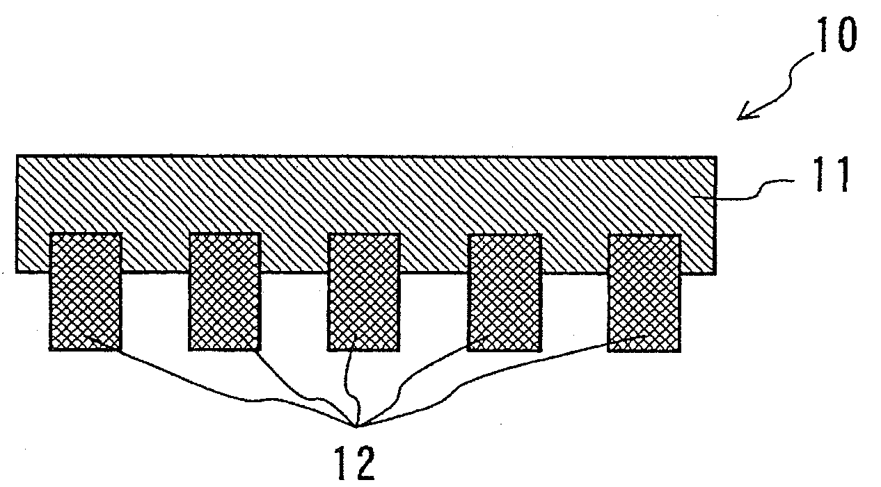
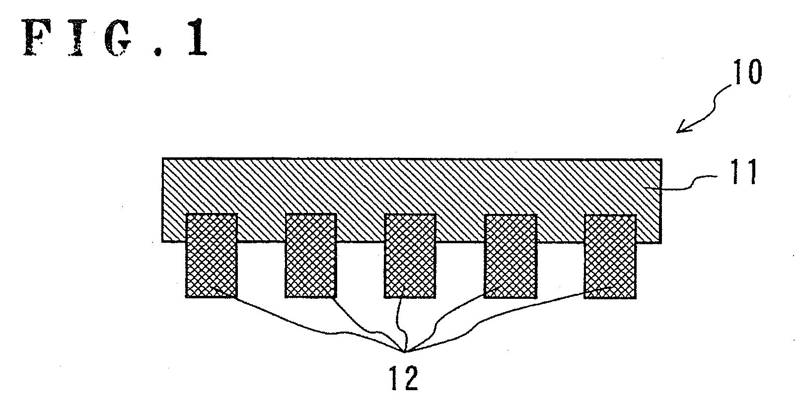
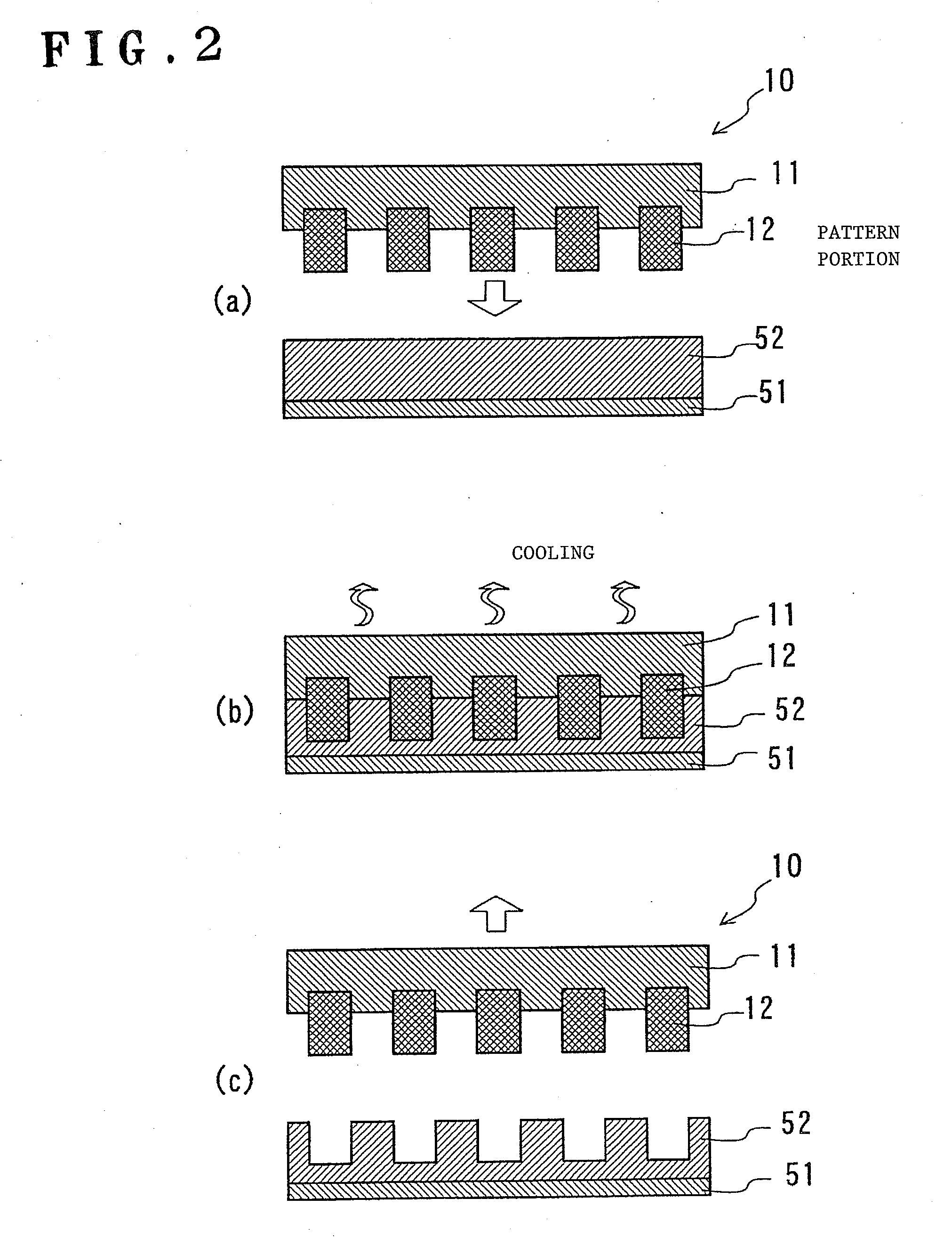
[0030]FIG. 1 shows a summary cross-sectional view of the mold 10 of a first embodiment of the invention. The mold 10 comprises a base portion 11, having a flat main face, and a pattern portion 12, provided so as to protrude from the main face of the base portion 11; by this means, the pattern portion 12 forms a relief shape in the main face of the base portion 11. The mold 10 of the first embodiment is characterized in being used for transfer when the molten-state resin film is a thermoplastic resin, and in particular, when transfer by thermal nanoimprinting is used.

[0031]Here, a transfer method using thermal nanoimprint processing is described in summary, referring to FIG. 2A through FIG. 2C. As shown in FIG. 2A, a PMMA (polymethyl methacrylate), polycarbonate, acrylic, or other thermoplastic resin 52 is applied by spin coating or another thin film formation means onto a substrate 51 comprising Si or another semiconductor. Then, the substrate 51 with the resin 52 applied is heated ...

second embodiment

[0042]Next, the mold 110 of a second embodiment of the invention is described, referring to FIG. 7. The mold 110 comprises a base portion 111 having a flat main face, and a pattern portion 112 provided so as to protrude from the main face of the base portion 111; by this means the pattern portion 112 forms a relief shape in the main face of the base portion 111. The mold 110 of the second embodiment is characterized in being used for transfer, and in particular for transfer by photo-nanoimprint transfer methods, when the molten-state resin film is a photo-curing resin. Here, a transfer method using photo-nanoimprint processes is described in summary referring to FIG. 8A through FIG. 8C.

[0043]First, as shown in FIG. 8A, a photohardening resin 152, comprising an epoxy, silicone, polyimide, or similar, is applied by a spin coater or other thin film formation means onto a substrate 151 comprising Si or another semiconductor. Next, as shown in FIG. 8B, a mold 110 is pressed with a pressu...


PUM

PropertyMeasurementUnit
Electrical resistanceaaaaaaaaaa
Shapeaaaaaaaaaa
Areaaaaaaaaaaa

Abstract

A mold of this invention comprises a base portion, and a pattern portion provided so as to protrude from a main face of the base portion, the base portion and the pattern portion being formed from different materials. By this means, a mold with the rigidity to withstand pressing forces during pattern transfer is provided.

Description

TECHNICAL FIELD[0001]This invention relates to a mold to form patterns in a resin film using an imprinting method.BACKGROUND ART[0002]Nanoimprint processes are attracting attention as technology for mass production of high-density semiconductor devices, magnetic recording devices, MEMS, next-generation recording media, and other fine-machined items. In this technology, by curing a resin in a molten state applied onto a substrate while pressing on the resin with a mold (transfer die), a relief shape with dimensions of several tens to several hundreds of nm, formed in one face of the mold, is transferred to the resin. Methods are broadly divided into thermal nanoimprint methods and photo-nanoimprint methods, according to the method of resin curing used (see, Patent Reference 1 and Non-patent Reference 1).[0003]In the above-described nanoimprint processes, when pressing the pattern face of the mold against the resin during transfer, the relief pattern of the pattern portion is sometime...

Claims


Application Information

Patent Timeline
IPC IPC(8): B29C43/02B81C99/00
CPCB29C33/38B29C33/42B29C59/022B29C2791/006B81C99/009H01L21/0273B82Y40/00G03F7/0002G11B5/743G11B5/82G11B5/855B82Y10/00
Inventor KATSUMURA, MASAHIRO
Owner PIONEER CORP
Why Eureka
Try Eureka