
Within-sequence metrology based process tuning for adaptive self-aligned double patterning

a self-aligning, process tuning technology, applied in the direction of fluid pressure measurement, semiconductor/solid-state device testing/measurement, instruments, etc., can solve the problems of reducing the spacing between features, cd reduction comes at the expense of dp methods, and is potentially cost prohibitiv

Inactive Publication Date: 2010-01-14
APPLIED MATERIALS INC
View PDF8 Cites 33 Cited by
  • Summary
  • Abstract
  • Description
  • Claims
  • Application Information

AI Technical Summary

Benefits of technology

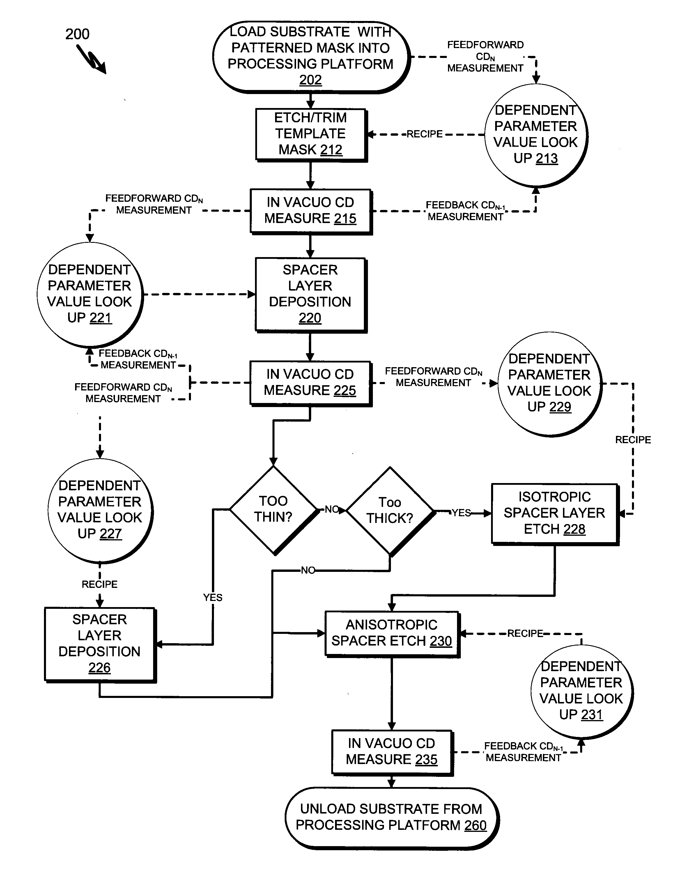
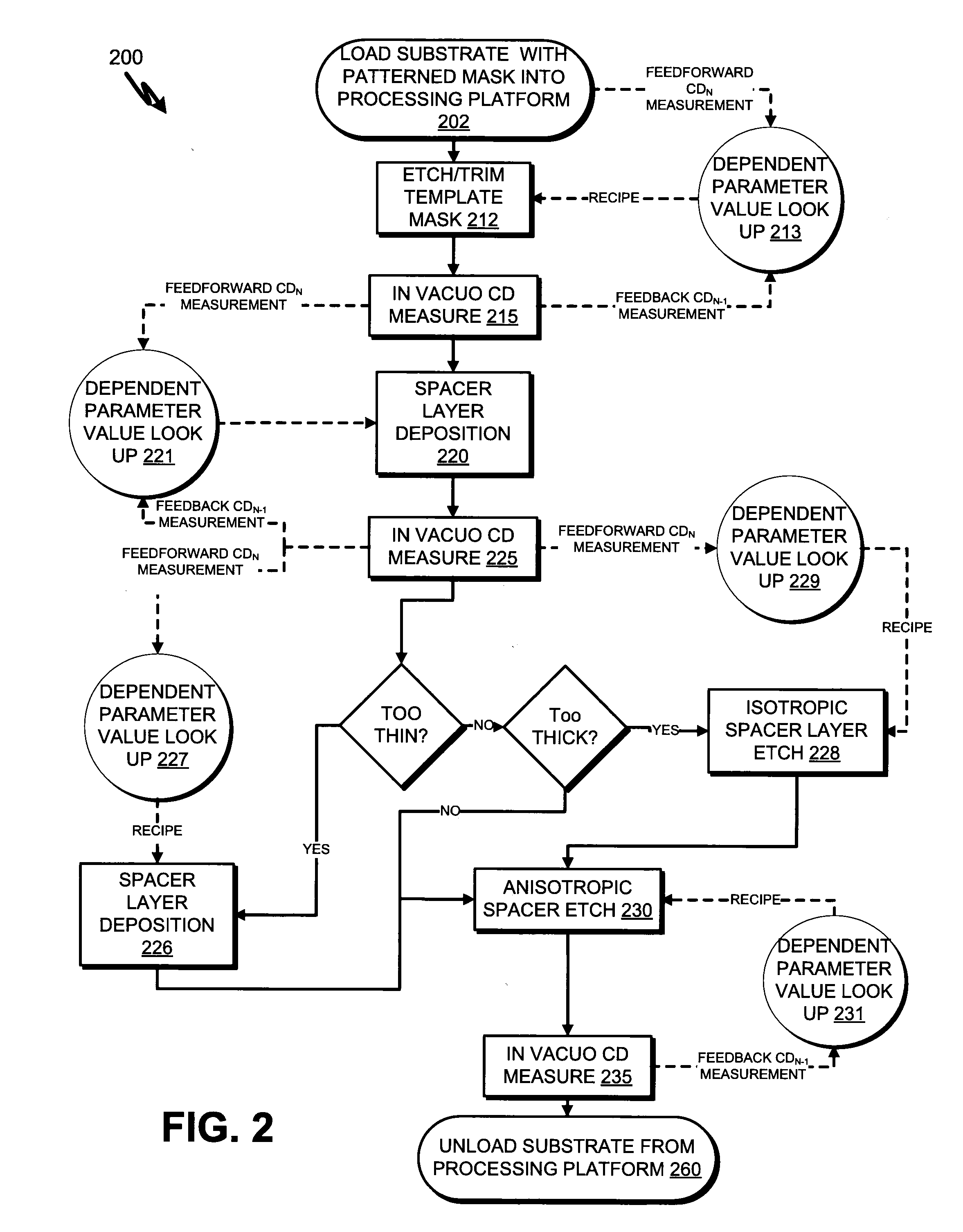
The present invention provides methods for tuning a process for making semiconductor devices using a technique called adaptive self-aligned dual patterning (SADP). The methods involve using in-vacuo metrology, such as in-vacuo optical CD (OCD) measurement, to gather feedback and feedforward parameters for adaptively determining the chamber sequence or adjusting process parameters in the SADP process. The in-vacuo CD measurement is performed between process operations and provides feedback for adaptively determining the chamber sequence or adjusting process parameters. The methods also involve depositing a layer of material over a template mask and etching the material to form a spacer, which is used to adjust the process parameters for subsequent operations. The in-vacuo CD measurement is used to determine the deposited layer thickness and based on this measurement, process parameters such as process time, process gas flow, power ratio, and temperature ratio are adjusted. The methods also involve using a plasma processing platform with a transfer chamber, process chambers for etch and deposition, and a metrology unit for in-vacuo CD measurement. The controllers process substrates through the process chambers and determine deposition process parameters based on the CD measurement from the metrology unit. The technical effects of the invention include improved accuracy and efficiency in the SADP process and better quality semiconductor devices.

Problems solved by technology

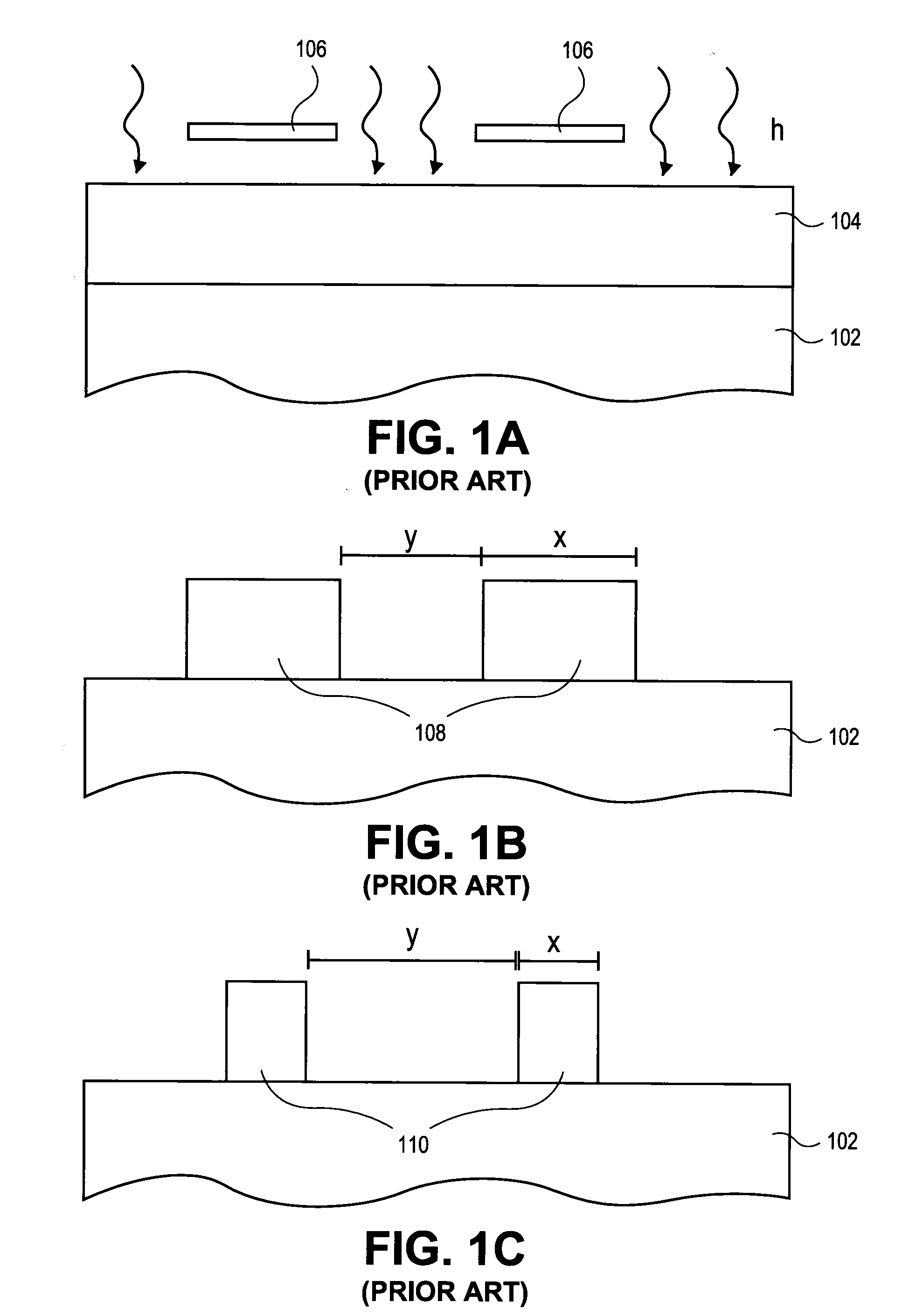
However, this reduction in feature CD comes at the expense of an increased spacing between features, as depicted by spacing ‘y’ in FIG. 1C.
DP methods however are potentially cost prohibitive, particularly as a result of production cycle time, which increases when a DP method employs many additional operations to pattern a particular layer.

Method used


Image

  • Within-sequence metrology based process tuning for adaptive self-aligned double patterning
  • Within-sequence metrology based process tuning for adaptive self-aligned double patterning
  • Within-sequence metrology based process tuning for adaptive self-aligned double patterning

Examples


Embodiment Construction

[0019]Reference throughout this specification to “an embodiment” means that a particular feature, structure, material, or characteristic described in connection with the embodiment is included in at least one embodiment of the invention. Thus, the appearances of the phrase “in an embodiment” in various places throughout this specification are not necessarily referring to the same embodiment of the invention. In the following description, numerous specific details are set forth, such as fabrication conditions and materials, to provide a thorough understanding of the present invention. However, particular embodiments may be practiced without one or more of these specific details, or in combination with other known methods, materials and apparatuses. Furthermore, the particular features, structures, materials, or characteristics described may be combined in any suitable manner in one or more embodiments. It should also be understood that specific embodiments may be combined where not m...


PUM

PropertyMeasurementUnit
magnetic fieldaaaaaaaaaa
temperatureaaaaaaaaaa

Abstract

An apparatus for adaptive self-aligned dual patterning and method thereof. The method includes providing a substrate to a processing platform configured to perform an etch process and a deposition process and a metrology unit configured for in-vacuo critical dimension (CD) measurement. The in-vacuo CD measurement is utilized for feedforward adaptive control of the process sequence processing platform or for feedback and feedforward adaptive control of chamber process parameters. In one aspect, a first layer of a multi-layered masking stack is etched to form a template mask, an in-vacuo CD measurement of the template mask is made, and a spacer is formed, adjacent to the template mask, to a width that is dependent on the CD measurement of the template mask.

Description

BACKGROUND[0001]1) Field[0002]Embodiments of the present invention pertain to the field of Semiconductor Processing and, in particular, to self-aligned double patterning (SADP).[0003]2) Description of Related Art[0004]FIGS. 1A-C illustrate cross-sectional views of a conventional semiconductor lithographic process. Referring to FIG. 1A, a photoresist layer 104 is provided above a semiconductor stack 102. A mask or reticle 106 is positioned above photoresist layer 104. A lithographic process includes exposure of photoresist layer 104 to radiation (hν) having a particular wavelength (λ), as indicated by the arrows in FIG. 1A. Referring to FIG. 1B, photoresist layer 104 is subsequently developed to remove the portions photoresist layer 104 that were exposed to light and thereby provide patterned photoresist layer 108 above semiconductor stack 102. The width of each feature of patterned photoresist layer 108 is depicted by the width ‘x’ of a feature and the space ‘y’ between each feature...

Claims


Application Information

Patent Timeline
Patent Type & Authority Applications(United States)
IPC IPC(8): H01L21/00C23F1/00
CPCB82Y10/00H01L21/0337H01L21/0338H01L21/67069H01L21/67207H01L2924/0002H01L22/12H01L22/20H01L21/67253H01L2924/00H01L21/0273
Inventor DAVIS, MATTHEW F.LILL, THORSTEN B.LIAN, LEI
Owner APPLIED MATERIALS INC
Learn More