Method And Device For Wetting The Bumps Of A Semiconductor Chip With Soldering Flux

Inactive Publication Date: 2010-01-28
BAUMANN DAMIAN +2
View PDF1 Cites 6 Cited by
  • Summary
  • Abstract
  • Description
  • Claims
  • Application Information

AI Technical Summary

Benefits of technology

[0007]The present invention is based on the object of developing a de

Problems solved by technology

This measure brings about that the front wall of the container does not convey any soldering flux

Method used


Image

  • Method And Device For Wetting The Bumps Of A Semiconductor Chip With Soldering Flux
  • Method And Device For Wetting The Bumps Of A Semiconductor Chip With Soldering Flux
  • Method And Device For Wetting The Bumps Of A Semiconductor Chip With Soldering Flux

Examples


example 1

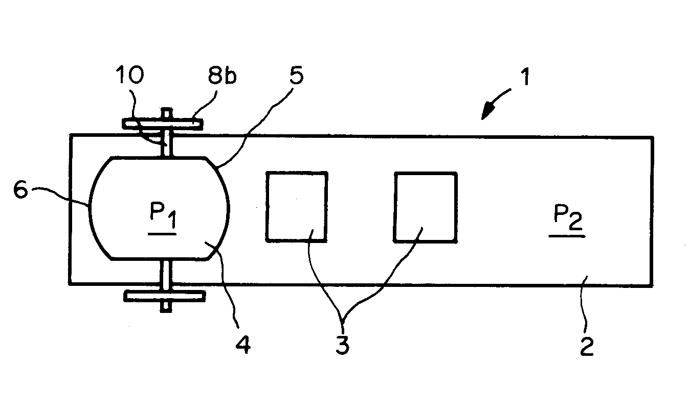
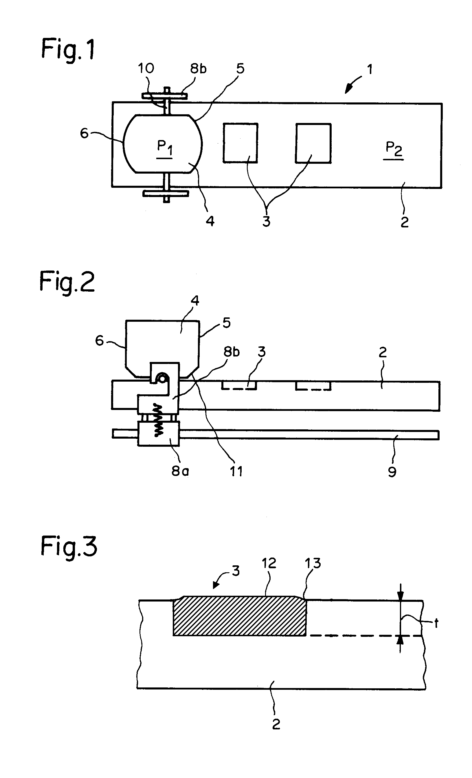
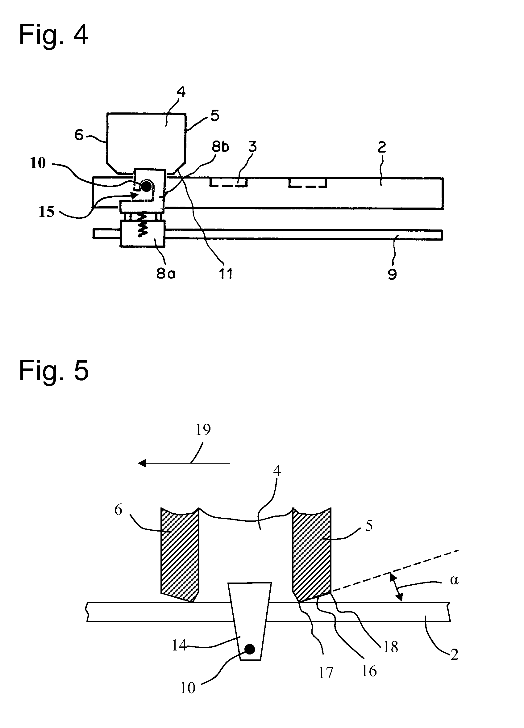
[0022]In this example, the drive known from CH 694634 is modified in such a way that the drive exerts a torque on the container 4, so that the front wall is automatically lifted up from the base plate 2 during the movement. As described above, the container 4 is driven by the slide formed by the bottom and the top slide parts 8a and 8b, in which the container 4 is removably mounted. The modifications of the drive are obvious from FIG. 4, which shows the modified drive in a lateral view. A plate 14 (not visible in FIG. 4, but implemented as in the example of FIG. 5), is attached in each case to the two side walls, which projects downward laterally adjacent the base plate 2. The plates 14 contain pins 10, which engage in a recess 15 in the top slide part 8b situated below the level of the top side of the base plate 2. The spring pulls the top slide part 8b downward against the guide rail 9. When the bottom slide part 8a is moved along the guide rail 9, the top slide part 8b exerts a f...

example 2

[0023]This example is based on the preceding example, but the lower edges of the walls 5 and 6 of the container 4, which are each alternately the front or rear wall, are implemented in such a way that the container 4 comes to rest on a surface 16 upon tilting. FIG. 5 shows a possible solution. If the drive moves the container 4 in the direction identified by the arrow 19, the force being transmitted at the pin 10, the wall 6 is the front wall and the wall 5 is the rear wall. The lower edge of such a wall 5, 6 comprises an inner edge 17 and an outer edge 18, which delimit the cited surface 16. In the rest state, the container 4 lies on the inner edges 17 of the front and rear wall. The surface 16 runs slightly diagonally upward at a predetermined angle a originating from the inner edge 17 to the outer edge 18, so that the outer edge 18 does not contact the base plate 2 in the rest state of the container 4. During the movement, the container 4 tilts as a result of the force engaging a...

example 3

[0024]In this example, the force generated by the drive engages above the base plate 2. A top slide part 8b is also provided here. FIG. 6, which is not drawn to scale, shows the front and rear walls 6, 5 of the container 4 in a sectional view. The section plane runs perpendicularly to the base plate 2 and parallel to the movement direction of the container 4 represented by an arrow 19. The front and the rear walls have a lower edge which is narrower than the thickness of the wall. The walls have a surface 21 running diagonally upward on their exterior side 20. The top slide part 8b has surfaces diametrically opposite this surface 21 having the same angle of inclination. The top slide part 8b additionally contains a projection 23 having a groove 24, into which the top end of the front or rear wall projects. If the slide is moved in the direction of the arrow, the top slide part 8b exerts a torque on the container 4, which causes the container 4 to tilt around the lower edge of the re...


PUM

PropertyMeasurementUnit
Heightaaaaaaaaaa
Distanceaaaaaaaaaa
Frictionaaaaaaaaaa

Abstract

The present invention relates to a method and a device for wetting the bumps of a semiconductor chip with a soldering flux, in which a container, which accommodates the soldering flux and is open on the bottom, and a base plate, which contains at least one cavity, are moved back-and-forth in relation to one another on one side of the cavity to the other side of the cavity. The viewed in the movement direction front wall of the container is lifted up during the relative movement, so that it is located at a distance above the base plate. The distance is somewhat greater than the height difference by which the soldering flux projects above the level of the surface of the base plate. This measure has the effect that the front wall of the container does not convey any soldering flux onto the base plate, which has caused the loss of this soldering flux until now.

Description

CROSS REFERENCE TO RELATED APPLICATIONS[0001]The present application is related to and claims priority of the PCT patent application no. PCT / EP2007 / 059545 entitled “Method And Device For Wetting Bumps Of A Semiconductor Chip With Soldering Flux”, filed Sep. 11, 2007, which in turn claims priority of Swiss patent application no. 1506 / 06, filed on Sep. 21, 2006, the disclosure of which is herein incorporated by reference.TECHNICAL FIELD[0002]The present invention relates to a method and a device for wetting the bumps of a semiconductor chip with soldering flux.BACKGROUND OF THE INVENTION[0003]For mounting semiconductor chips a technology is widespread in which the semiconductor chips are initially attached to a substrate using a so-called die bonder. Subsequently, the electrical connection areas of the semiconductor chip are wired to the substrate using a so-called wire bonder. Another technology is flip chip technology, in which the connection areas of the semiconductor chip are prov...

Claims


Application Information

Patent Timeline
IPC IPC(8): B23K1/20B23K3/08
CPCB23K1/203B23K2201/40H01L2224/11822H01L2924/01068H01L21/6715B23K2101/40B23K1/20B23K3/08
Inventor BAUMANN, DAMIANGRUETER, RUEDIWERNE, DOMINIK
Owner BAUMANN DAMIAN
Why Eureka
Try Eureka