
Solid-state image sensing device, method and apparatus for manufacturing same, and electronic device

Active Publication Date: 2010-01-28
SHARP KK
View PDF6 Cites 7 Cited by
  • Summary
  • Abstract
  • Description
  • Claims
  • Application Information

AI Technical Summary

Benefits of technology

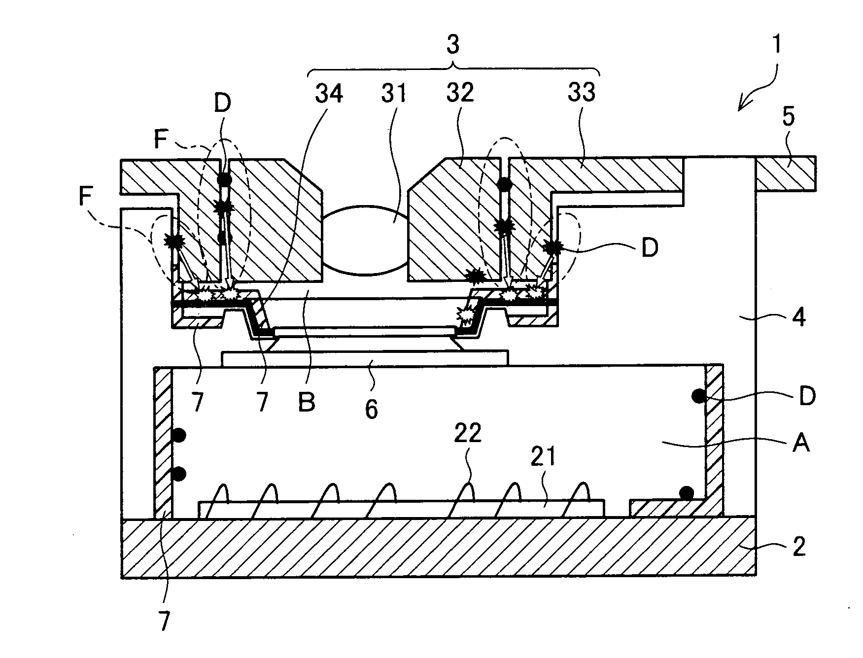
[0024]The present invention, conceived in view of the problems, has an objective of providing a solid-state image sensing device capable of preventing image defects from occurring due to dust produced during manufacture and while in use and also providing a method and apparatus for manufacturing the solid-state image sensing device, and an electronic device incorporating the solid-state image sensing device.
[0066]An electronic device according to the present invention includes any one of the foregoing solid-state image sensing devices. The resultant electronic device reduces image defects because it includes a solid-state image sensing device.

Problems solved by technology

These conventional structures have an inherent problem that none of them is completely free from image defects.
The dust results in a defective image.
In the structure of Patent Literature 4, dust can still attach in the optical path in this manner, causing an defect in images.

Method used


Image

  • Solid-state image sensing device, method and apparatus for manufacturing same, and electronic device
  • Solid-state image sensing device, method and apparatus for manufacturing same, and electronic device
  • Solid-state image sensing device, method and apparatus for manufacturing same, and electronic device

Examples


Embodiment Construction

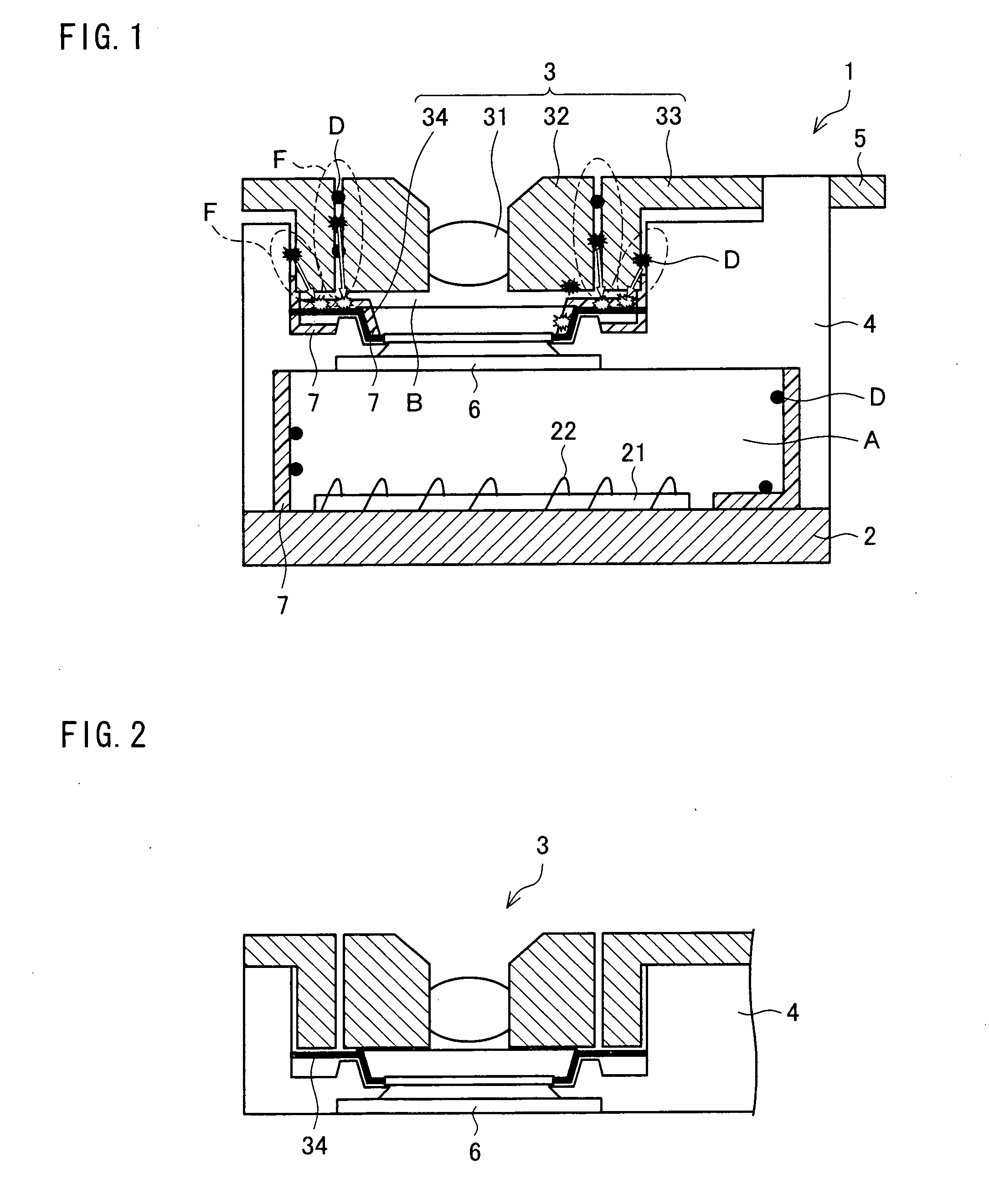
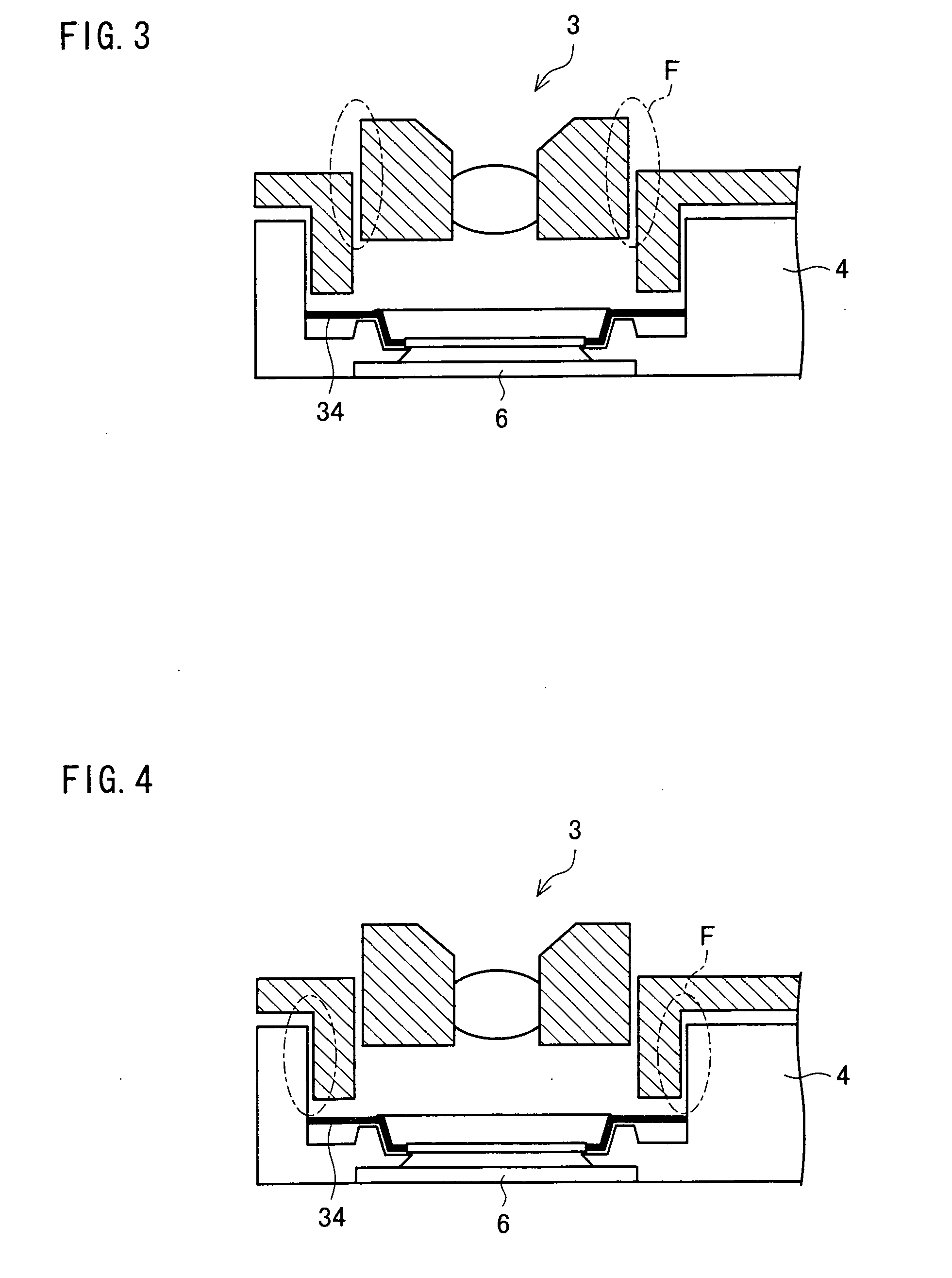
[0125]An embodiment of the present invention will be described in reference to FIGS. 1 to 16.

1. Solid-State Image Sensing Device According to Present Invention

[0126]The solid-state image sensing device according to the present invention is characterized in that image defects are reduced by collecting dust in grease.

[0127]The solid-state image sensing device according to the present invention is suitable for use in electronic devices with image sensing function, including mobile camera phones, digital still cameras, and security cameras. The present embodiment will describe a camera module (solid-state image sensing device) incorporated in a mobile camera phone.

[0128]FIG. 6 is an oblique view of the camera module of the present embodiment, illustrating its appearance. The camera module 1 integrally contains a wiring board 2, an optical structure 3, a lens holder 4, and a lever 5 as illustrated in FIG. 6. The lens holder 4, in which the image sensing optical structure 3 is accommodate...


PUM


Abstract

A camera module (1) is an assembly of a lens holder (4) and a wiring board (2). The lens holder (4) holds an optical structure (3) which forms an image of a subject. The wiring board (2) has formed thereon a solid-state image sensing element (21) which converts the image of the subject formed by the optical structure (3) to electrical signals. Grease (7) is applied to the camera module (1) in such a manner that the grease is not present in an optical path in the optical structure (3). The grease (7) catches the dust (D) produced during manufacture and while in use, thereby prevented the dust (D) from causing image defects. A solid-state image sensing device is thus provided which is capable of preventing the dust produced during manufacture and while in use from causing image defects.

Description

TECHNICAL FIELD [0001]The present invention relates to solid-state image sensing devices capable of preventing dust from attaching to an optical path during manufacture and while in use and relates also to methods and apparatus for manufacturing such a device and electronics incorporating the device.BACKGROUND ART [0002]An image sensing camera module (solid-state image sensing device) mounted, for example, to mobile phones integrally contains a solid-state image sensing element, an infrared filter, a wiring board with terminals, a lens, and a lens holder. The solid-state image sensing element may be a CCD (charge-coupled device) or a CMOS (complementary metal-oxide semiconductor) sensor IC (integrated circuit). Manufacturing processes have been progressively adapted for reducing the size of the solid-state image sensing element in step with the reduction in size of the camera module. In the increasingly more compact camera modules, fine dust (for example, 25 μm or larger) on an opti...

Claims


Application Information

Patent Timeline
IPC IPC(8): H01L31/0203H01L31/0232B05D5/12B05C5/00B05C1/00H04N5/225
CPCH04N5/2257H04N5/2251H04N23/52H04N23/57H04N23/55
Inventor TSUKAMOTO, HIROAKIKINOSHITA, KAZUO
Owner SHARP KK
Learn More