

Packaging structure for integration of microelectronics and MEMS devices by 3D stacking and method for manufacturing the same
- Summary
- Abstract
- Description
- Claims
- Application Information
AI Technical Summary
Problems solved by technology
Method used
Image

Examples
Embodiment Construction
[0028]The present invention can be exemplified by the preferred embodiments as described hereinafter.
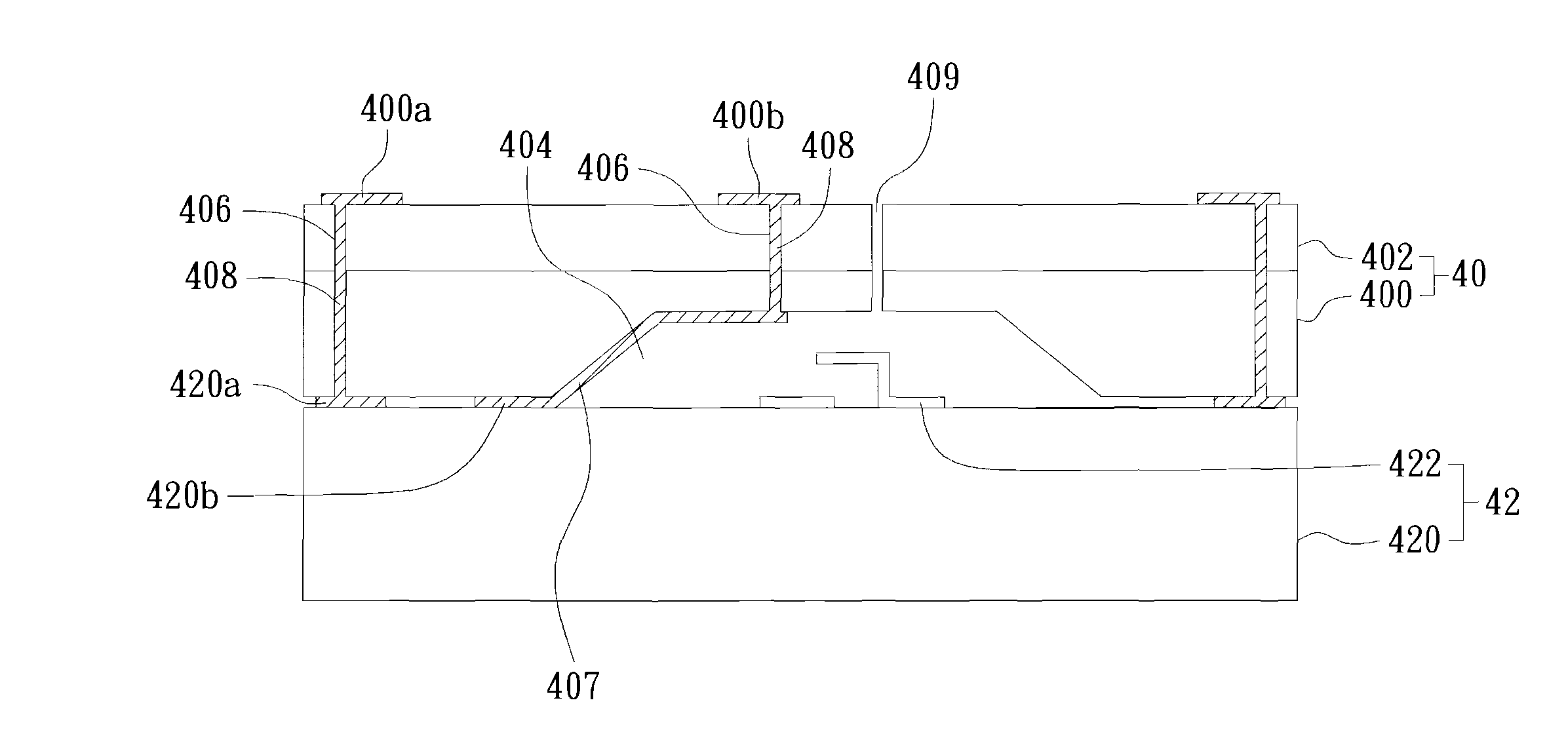
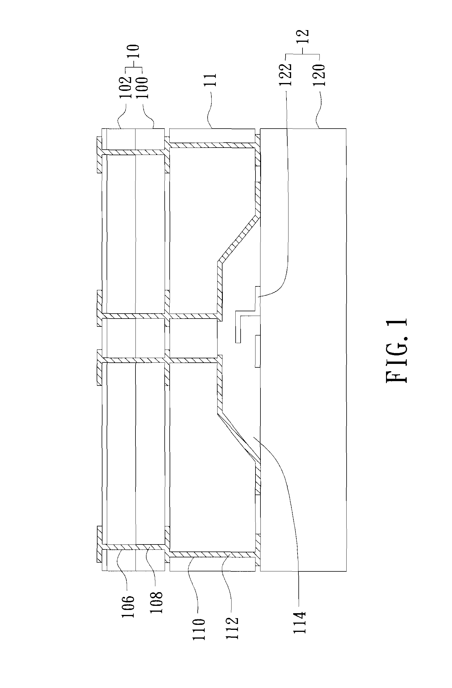
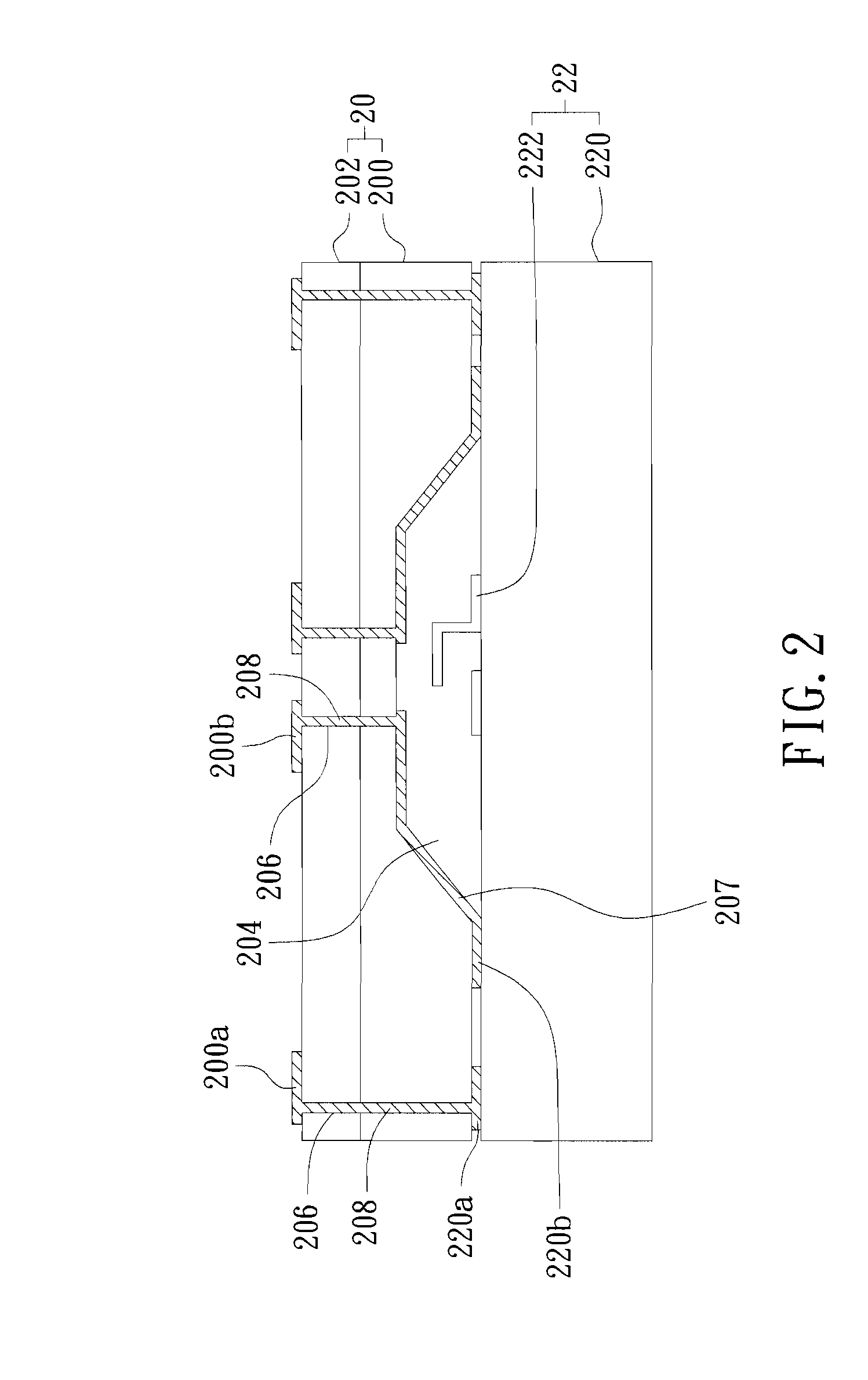
[0029]Please refer to FIG. 2, which is a cross-sectional view of a packaging structure for integration of microelectronics and MEMS devices by three-dimensional (3D) stacking according to the present invention. In FIG. 2, the packaging structure comprises an ASIC unit 20 and a MEMS unit 22. The ASIC unit 20 is stacked on the MEMS unit 22. The ASIC unit 20 comprises a substrate 200 and a circuit layout 202 disposed on a surface of the substrate 200. To achieve electrical connection, the ASIC unit 20 comprises a plurality of through holes 206 and the through holes 206 are filled with a conductive material 208, which can be a metal material such as copper (Cu). The MEMS unit 22 comprises a substrate 220 and a micro sensor 222 disposed on a surface of the substrate 220. However, the present invention is different from the prior art in that a cavity 204 is provided on a surface of the sub...
PUM
| Property | Measurement | Unit |
|---|---|---|
| Electrical conductor | aaaaa | aaaaa |
Abstract
Description
Claims
Application Information