Product Optimization Process for Embedded Passives

a passive component and product optimization technology, applied in the field of multi-layer circuit board manufacturing, can solve the problems of limiting the precision of the components that can be formed, the value of embedded passive components that are formed on the board is not uniform, and the design and etching process can also introduce errors, so as to improve the accuracy of analysis

Inactive Publication Date: 2010-02-04
HARRIS CORP
View PDF17 Cites 3 Cited by
  • Summary
  • Abstract
  • Description
  • Claims
  • Application Information

AI Technical Summary

Benefits of technology

[0018]The measuring and the analyzing steps described herein can be repeated for each one of a plurality of the multi-layer circuit boards to be manufactured with a particular embedded circuit design. T

Problems solved by technology

However, the tolerances involved in such published values substantially limit the precision of the components that can be formed.
These broad tolerances can result in rather large variations in the value of the embedded passive components formed on the board, particularly when the material variations are combined with other manufacturing tolerance errors.
For example, the design and etching process can also introduce errors.
Adding passive component material to the etched board is not

Method used


Image

  • Product Optimization Process for Embedded Passives
  • Product Optimization Process for Embedded Passives
  • Product Optimization Process for Embedded Passives

Examples


Embodiment Construction

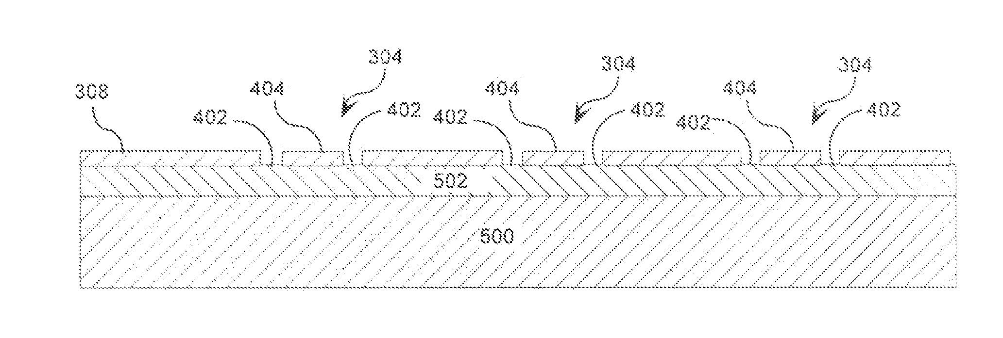
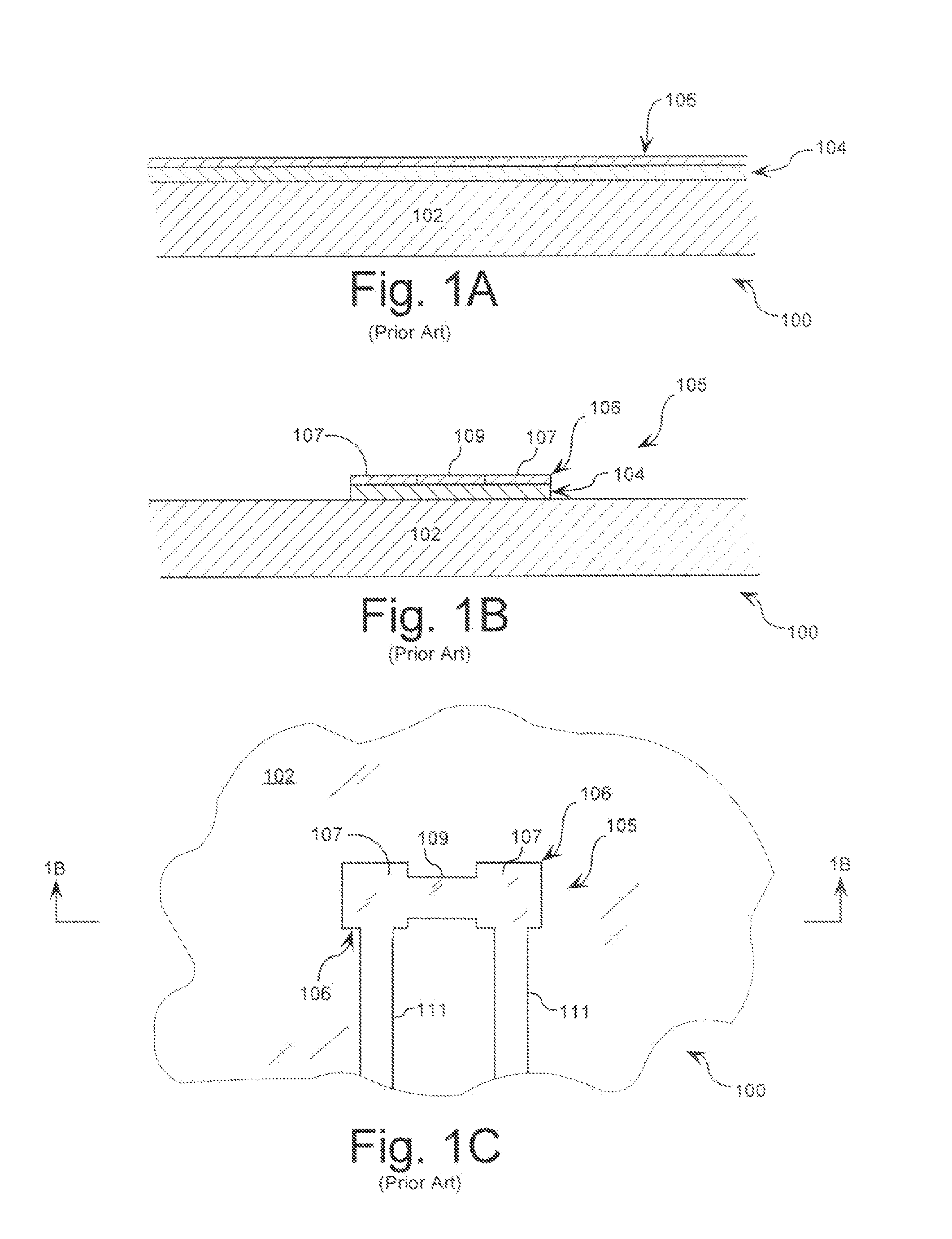
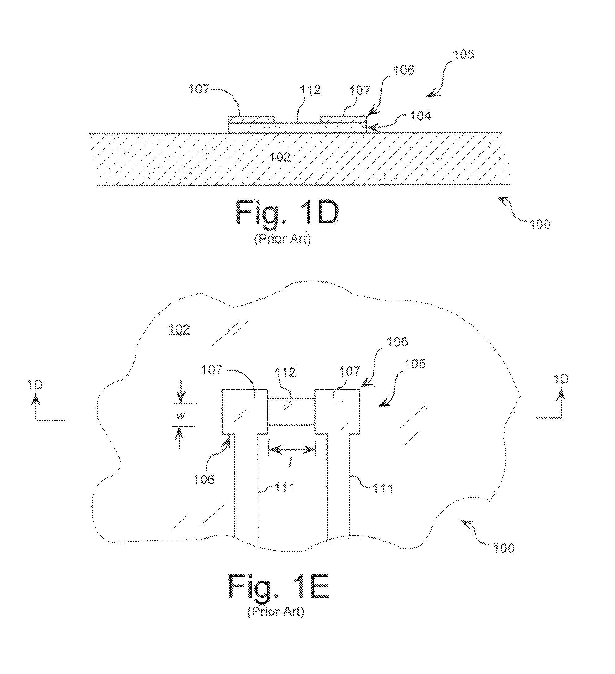
[0027]In order to assist the reader in understanding the inventive arrangements, a conventional process used to form embedded passive components in circuit boards will be described. This conventional process is illustrated in FIG. 1A-1G. The process begins by selecting a circuit board panel (“a board”) 100 as shown in FIG. 1A. The board 100 has a dielectric layer 102, a passive component layer 104, and a conductive metal layer 106. The dielectric layer can be comprised of a woven glass material, a non-woven glass material, or any other dielectric material known in the art. The passive component layer 104 is typically comprised of a passive component material suitable for fabricating resistors (“resistor material”) or for fabricating capacitors (“a capacitor material”). The resistor material can include a metal thin film on a copper foil, a polymer thick film, a ceramic thick film, or the like. The capacitor material can include, but is not limited to, a polyimide, a proprietary diel...


PUM

PropertyMeasurementUnit
Electrical resistanceaaaaaaaaaa
Electrical conductoraaaaaaaaaa
Areaaaaaaaaaaa

Abstract

A method is provided for manufacturing a multi-layer circuit board having embedded passive components. The method includes selectively removing portions of at least one layer of the multi-layer circuit board (300) to form a two dimensional array of test points (304) defining a grid extending across a surface of the multi-layer circuit board in those areas on which a circuit is to be formed. The method also includes measuring at each of the test points at least one electrical parameter which is useful for defining a characteristic of the multi-layer circuit board. The method further includes selectively modifying the geometry of at least one embedded passive component to be formed on the multi-layer circuit board based on an analysis of a result obtained in the measuring step.

Description

STATEMENT REGARDING FEDERALLY SPONSORED RESEARCH OR DEVELOPMENT[0001]This invention was made with government support under FA8650-06-C-5505 awarded by United States Air Force. The government has certain rights in the invention.BACKGROUND OF THE INVENTION[0002]1. Statement of the Technical Field[0003]The inventive arrangements relate to circuit boards. More particularly, the present invention relates to a method for manufacturing multi-layer circuit boards having interconnecting substrates and passive components embedded directly into the interconnecting substrates.[0004]2. Description of the Related Art[0005]There is a growing demand to design and manufacture smaller circuit boards having increased functionality. As such, a new circuit board technology has emerged. This circuit board technology deals with embedding passive components directly into circuit boards. This embedding is achieved by placing one or more passive components between two (2) interconnecting substrates of a circ...

Claims


Application Information

Patent Timeline
IPC IPC(8): H05K3/46H05K3/06H05K3/30
CPCH05K1/0268H05K1/16H05K1/162H05K1/167Y10T29/49165H05K3/46H05K2203/171Y10T29/4913Y10T29/49155H05K3/0005
Inventor BENDIX, LENDON L.
Owner HARRIS CORP
Why Eureka
Try Eureka