Waveguide grating structure and optical measurement arrangement

a waveguide grating and optical measurement technology, applied in the direction of waveguides, instruments, and analysis by subjecting materials to chemical reactions, can solve the problems of unsuitable focussing light field, unoptimized beam guiding, and inability to achieve simultaneous illumination of two-dimensional arrays of waveguide grating sensors

Inactive Publication Date: 2010-02-04
ARTIFICIAL SENSING INSTR ASI
View PDF31 Cites 32 Cited by
  • Summary
  • Abstract
  • Description
  • Claims
  • Application Information

AI Technical Summary

Benefits of technology

[0013](9) increases the measurement accuracy by way of scan averaging methods or resonance location averaging methods; and,

Problems solved by technology

The beam guiding, however, is not optimal.
The reflected light beam and the second incident light beam oppositely have the same direction, which may lead to perturbations.
A focussing light field is not suitable for simultaneous illumination of a two-dimensional array of waveguide grating sensors.
Furthermore, there is no mention of a method for temperature compensation in this application.

Method used


Image

  • Waveguide grating structure and optical measurement arrangement
  • Waveguide grating structure and optical measurement arrangement
  • Waveguide grating structure and optical measurement arrangement

Examples


Embodiment Construction

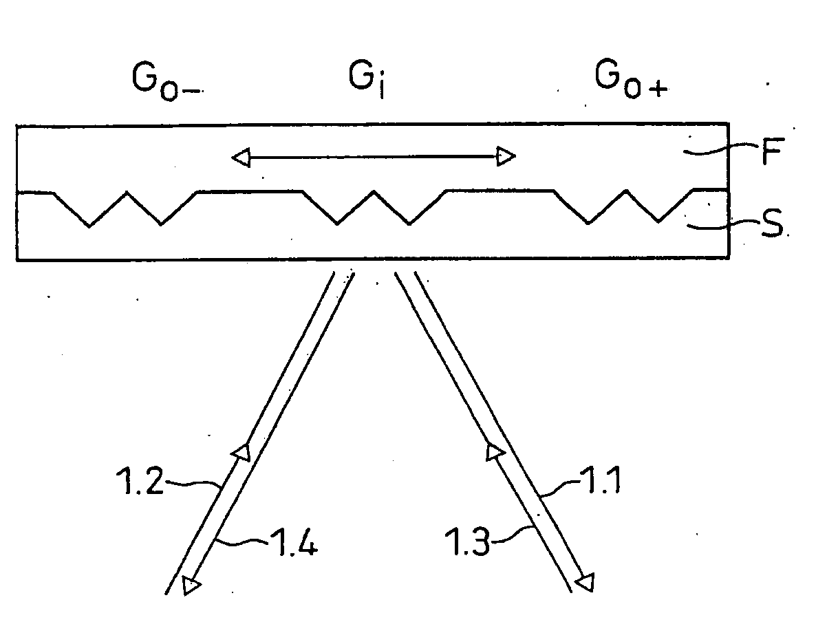
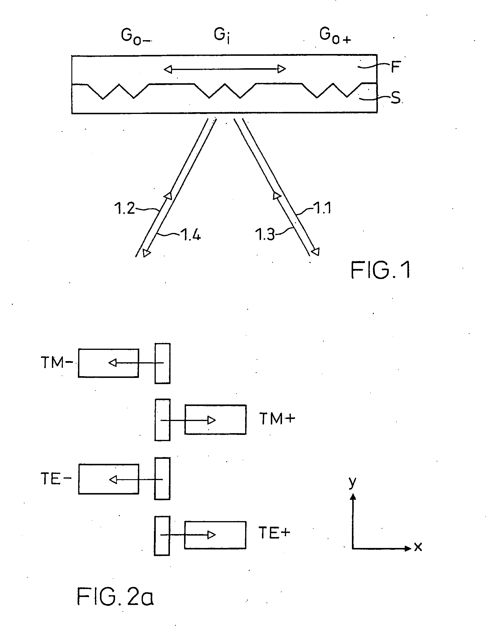
[0026]FIG. 1 shows a three-grating arrangement with a coincident beam guiding. The reflected beam 1.1 of the left incident light wave 1.2 runs directly opposite the right incident light wave 1.3 (with reflection beam 1.4). The middle grating is the in-coupling grating Gi. Located to the left and right of this are the two out-coupling gratings G0+ and G0−. The wave-guiding film F is located on the substrate S. The arrows in the wave-guiding film F represent the propagation direction of the modes. With a perpendicular incidence of light the reflected light beam indeed runs back in itself. If the light source is specially a laser source (laser diode source), then a coincident guiding of the beam may cause laser fluctuations since an external resonator is connected to the actual laser resonator. Laser fluctuations create instabilities in the measurement signal.

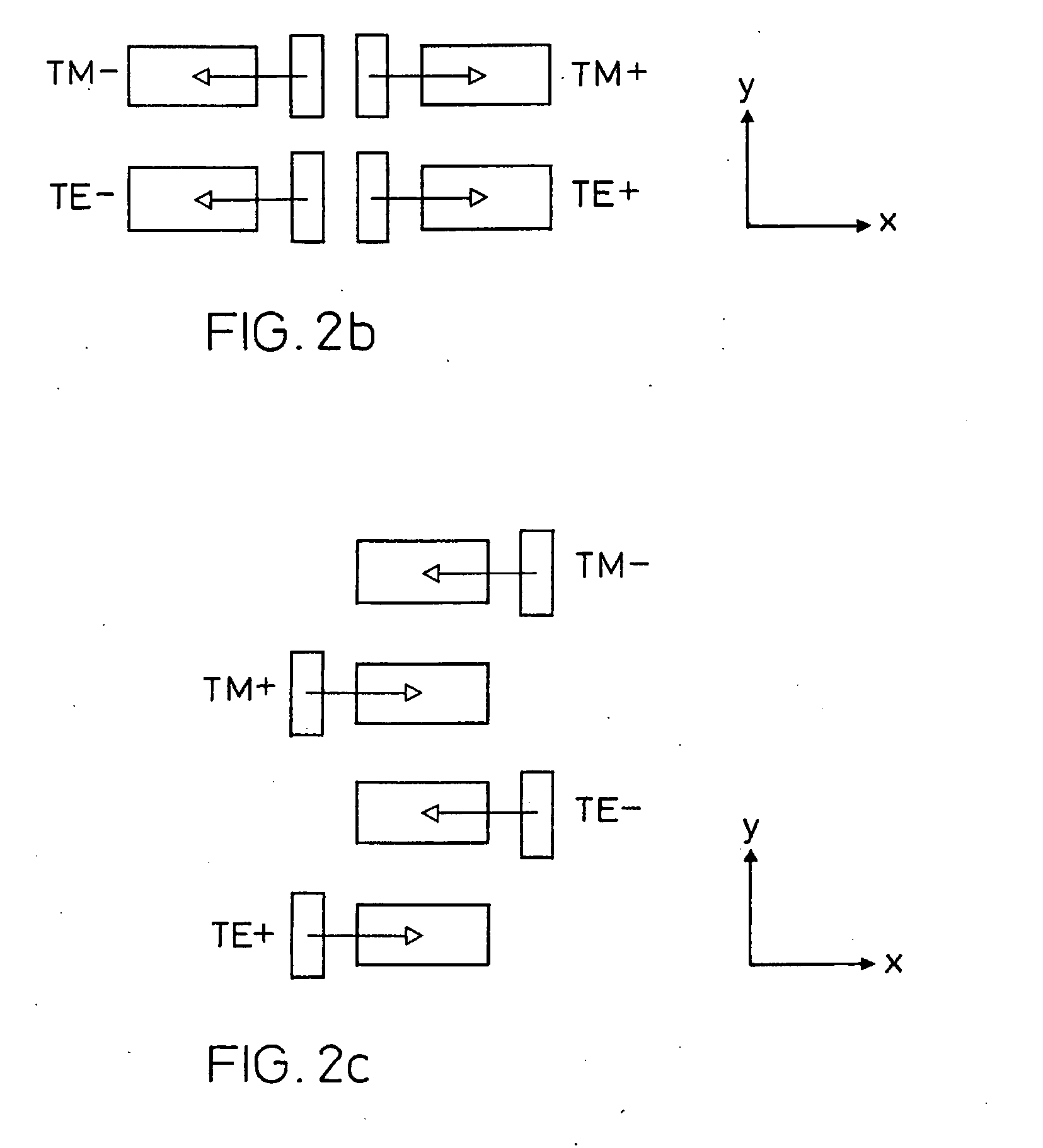
[0027]FIGS. 2a, 2b, and 2c show special waveguide grating structure units of a waveguide grating structure, wherein the small re...


PUM

PropertyMeasurementUnit
incident angleaaaaaaaaaa
thickaaaaaaaaaa
thicknessaaaaaaaaaa

Abstract

The present invention describes (bio)chemo-functional waveguide grating structures consisting of at least one (bio)chemo-functional waveguide grating structure unit or at least one (bio)chemo-functional sensor location with beam guidance permitting light beam separation, as well as detection methods for parallel analysis which are marking-free or based on marking.

Description

BACKGROUND OF THE INVENTION[0001]Various waveguide grating structures have already been described in the PCT applications PCT / EP94 / 02361 and PCT / CH98 / 00389. The beam guiding, however, is not optimal. The reflected beam of a first incident light wave coincides with the direction of a second incident light wave. The reflected light beam and the second incident light beam oppositely have the same direction, which may lead to perturbations. The PCT applications PCT / EP94 / 02361 and PCT / CH98 / 00389 do not illustrate how a waveguide grating sensor structure that consists of two-dimensionally arranged sensor locations may be read out in parallel in the case of detection free of marking. Parallel reading-out is, however, necessary in order to achieve a higher throughput.[0002]In the European patent application EP 0 482 377 A2 the waveguide grating is illuminated with a focussing light field. A focussing light field is not suitable for simultaneous illumination of a two-dimensional array of wav...

Claims


Application Information

Patent Timeline
Patent Type & Authority Applications(United States)
IPC IPC(8): G01R27/08G01N21/77G02B6/12
CPCG01N21/648G01N21/7743G01N21/6486G02B2006/12107Y10S385/901G01N33/54373G01N2021/6463G01N2201/08G02B6/124G02B6/32
Inventor TIEFENTHALER, KURT
Owner ARTIFICIAL SENSING INSTR ASI
Why Eureka
Try Eureka