Method of manufacturing organic light emitting device

Active Publication Date: 2010-02-04
SAMSUNG DISPLAY CO LTD
View PDF12 Cites 8 Cited by
  • Summary
  • Abstract
  • Description
  • Claims
  • Application Information

AI Technical Summary

Benefits of technology

[0008]Embodiments of the present invention provide a method of manufacturing an organic light emitting devi

Problems solved by technology

When forming the pixel defining layer, patterning is performed by using photolithography and wet etching so as to form openings for defining pixels, therefore a light emitting layer formed of an organic material may be damaged.
In addition, when the pixel defining layer is formed of an ino

Method used


Image

  • Method of manufacturing organic light emitting device
  • Method of manufacturing organic light emitting device
  • Method of manufacturing organic light emitting device

Examples


Embodiment Construction

[0023]The present invention will now be described more fully with reference to the accompanying drawings, in which exemplary embodiments of the present invention are shown.

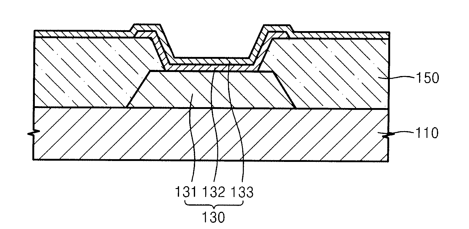
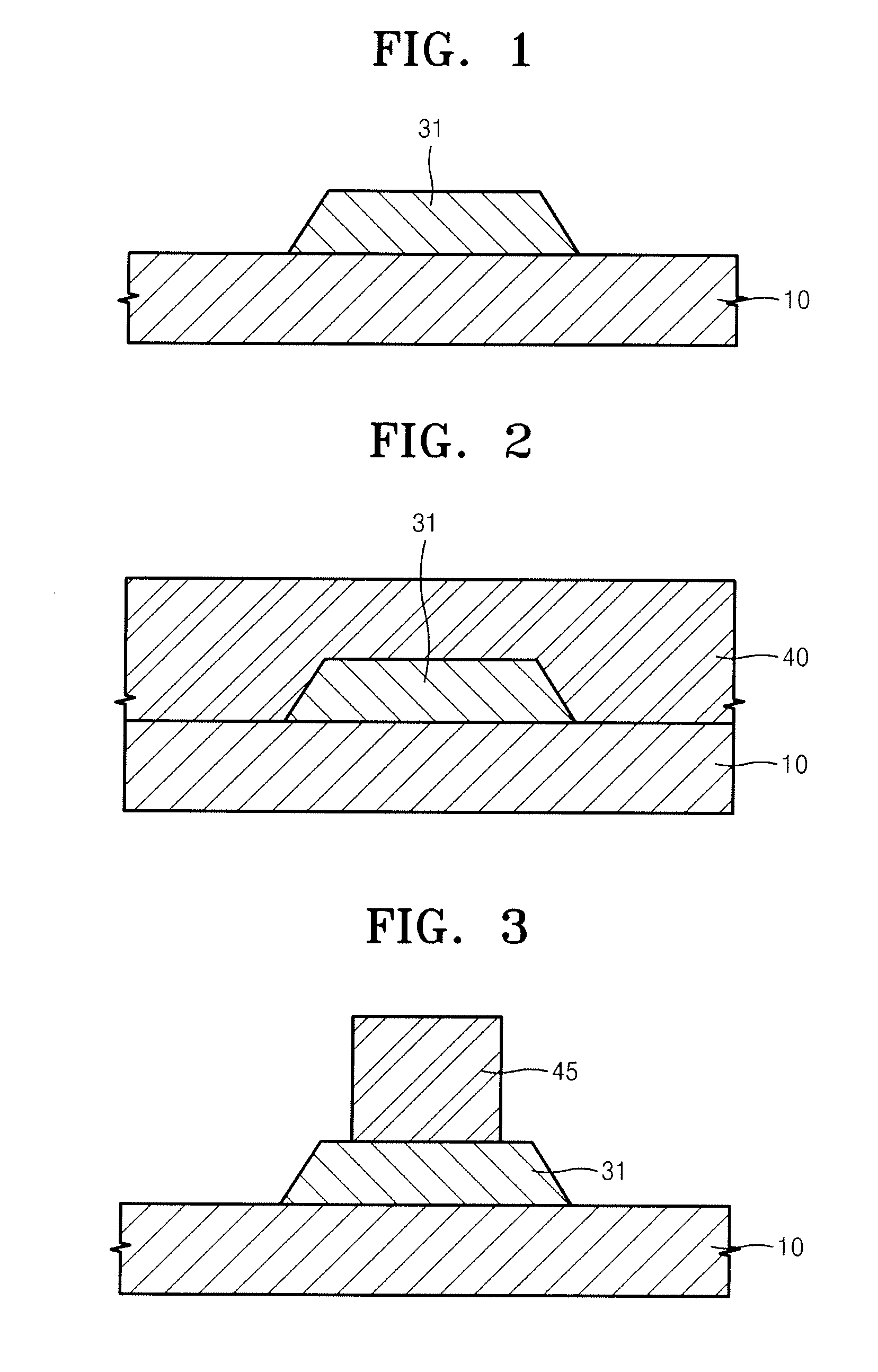
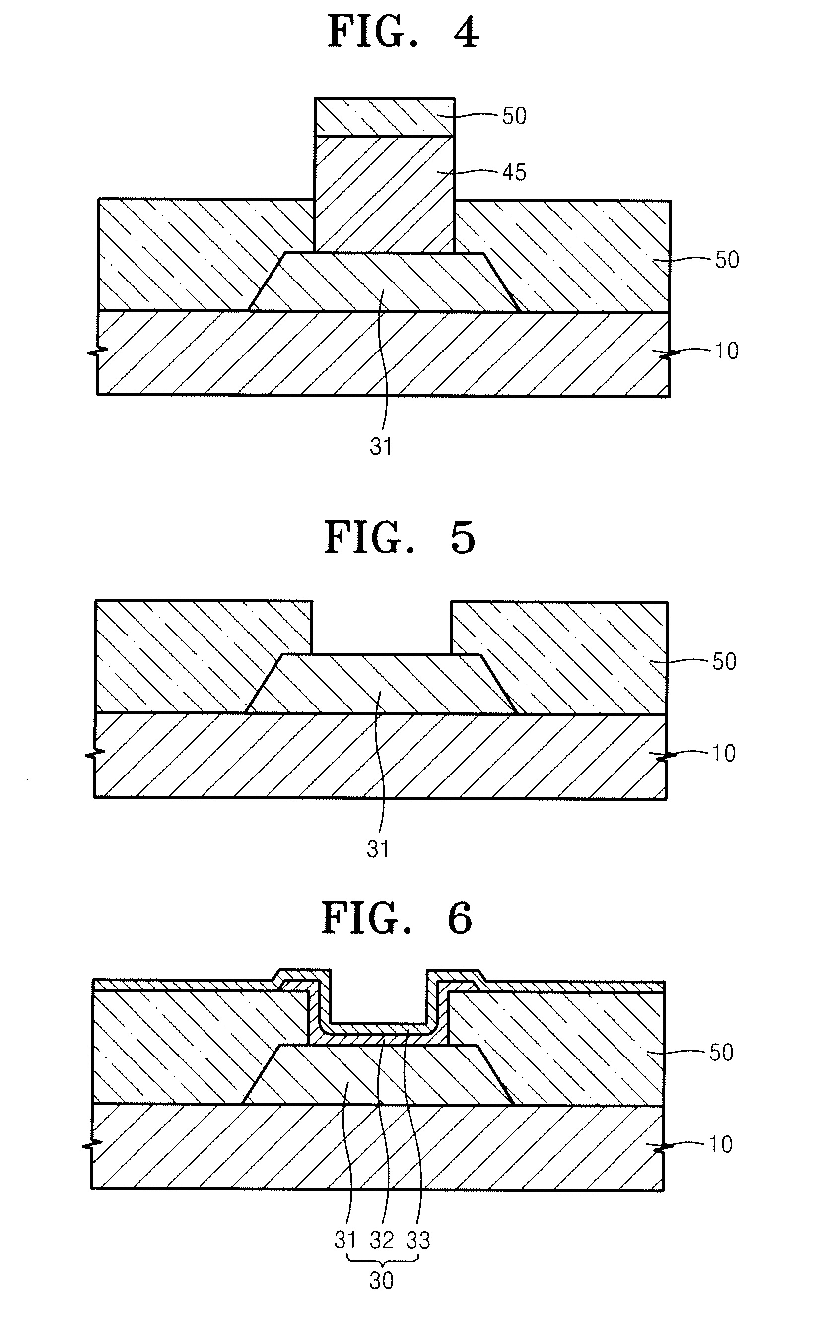
[0024]FIGS. 1 through 6 are schematic drawings illustrating cross-sectional views of an organic light emitting device for sequentially illustrating a method of manufacturing an organic light emitting device according to an embodiment of the present invention. The method of manufacturing an organic light emitting device according to the current embodiment includes forming a first electrode 31 on a substrate 10, forming a blocking layer 45 on the first electrode 31, forming a pixel defining layer 50 on the substrate 10, and sequentially forming an intermediate layer 32 and a second electrode 33 on the first electrode 31.

[0025]Referring to FIG. 1, the first electrode 31 is formed on the substrate 10. The substrate 10 may be formed of transparent glass mainly including SiO2. However, the present invention is not limit...


PUM


Abstract

A method of manufacturing an organic light emitting device by which a pixel defining layer can be easily formed. The method includes: forming a first electrode on a substrate; forming a photoresist layer to cover the first electrode; patterning the photoresist layer and forming a blocking layer so that the blocking layer is on a side of the first electrode opposite to a side facing the substrate; forming a pixel defining layer on the substrate to cover side ends of the first electrode; removing the blocking layer and exposing the side of the first electrode contacting the blocking layer; forming an intermediate layer including an organic light emitting layer on the side of the first electrode that is exposed by removing the blocking layer; and forming a second electrode on the intermediate layer.

Description

CROSS-REFERENCE TO RELATED PATENT APPLICATION[0001]This application claims priority to and the benefit of Korean Patent Application No. 10-2008-0074712, filed on Jul. 30, 2008, in the Korean Intellectual Property Office, the disclosure of which is incorporated herein in its entirety by reference.BACKGROUND OF THE INVENTION[0002]1. Field of the Invention[0003]The present invention relates to an organic light emitting device, and more particularly, to a method of manufacturing an organic light emitting device by which a pixel defining layer can be easily formed.[0004]2. Description of the Related Art[0005]Recently, display devices such as portable display devices and thin flat display devices have been developed. Field emission devices (FEDs), which are a type of flat display device, are self-luminescence display devices having a wide viewing angle, excellent contrast and fast response speed, and thus are considered as next generation display devices. In addition, organic light emitti...

Claims


Application Information

Patent Timeline
IPC IPC(8): H01L21/28
CPCH01L27/3246H01L51/56H01L27/3283H10K59/173H10K59/122H10K71/00H01L21/02107H01L21/76804H01L31/0264
Inventor SONG, ALEXYANG, NAM-CHOULSUH, MIN-CHULLEE, SEONG-TAEK
Owner SAMSUNG DISPLAY CO LTD
Why Eureka
Try Eureka