AI technical title is built by Patsnap AI team. It summarizes the technical point description of the patent document.
a memory system and non-volatile technology, applied in memory systems, memory adressing/allocation/relocation, instruments, etc., can solve the problems of increasing the complexity of flash memory with embedded controllers, affecting product diversification, product diversification, device performance, etc., to increase the chip size, increase the memory capacity, and reduce the size overhead of memory controller circuitry.
Inactive Publication Date: 2010-02-04
CONVERSANT INTPROP MANAGEMENT INC
View PDF101 Cites 24 Cited by
Summary
Abstract
Description
Claims
Application Information
AI Technical Summary
This helps you quickly interpret patents by identifying the three key elements:
Problems solved by technology
Method used
Benefits of technology
Benefits of technology
[0006]An embedded controller used to control access to a memory array contained in a chip typically increases the chip size from 15% to 30%. If multiple devices are integrated in a package to increase memory capacity, the size overhead associated with memory controller circuitry may become significant because controller circuitry is repeated on each of the multiple devices. Further, wafer yield (the number of working chips produced on a wafer) tends to be a function of chip size. The additional space required by one or more embedded controllers increases chip size, and thus may lead to a drop in overall wafer yield.
Problems solved by technology
If multiple devices are integrated in a package to increase memory capacity, the size overhead associated with memory controller circuitry may become significant because controller circuitry is repeated on each of the multiple devices.
The additional space required by one or more embedded controllers increases chip size, and thus may lead to a drop in overall wafer yield.
The increased complexity of a Flash memory with embedded controller can also have detrimental effects on product diversification, development time and cost, and device performance.
Such a device, in contrast to a discrete Flash memory, requires a more complex circuit layout, leading to longer development cycles.
Further, product redesign is also hindered because modifications to the design must be adapted to the entire chip.
Performance may also be degraded by this design.
A memory controller benefits from utilizing high-speed transistors; however, implementing both high-voltage and high-speed transistors on a single die can significantly increase manufacturing cost.
Thus, an embedded controller may instead utilize the high-voltage transistors required by the Flash memory, thereby slowing the performance of the controller.
Method used
Image
Click on the blue label to locate the original text in one second.
Reading with bidirectional positioning of images and text.
Examples
Embodiment Construction
[0024]A description of example embodiments of the invention follows.
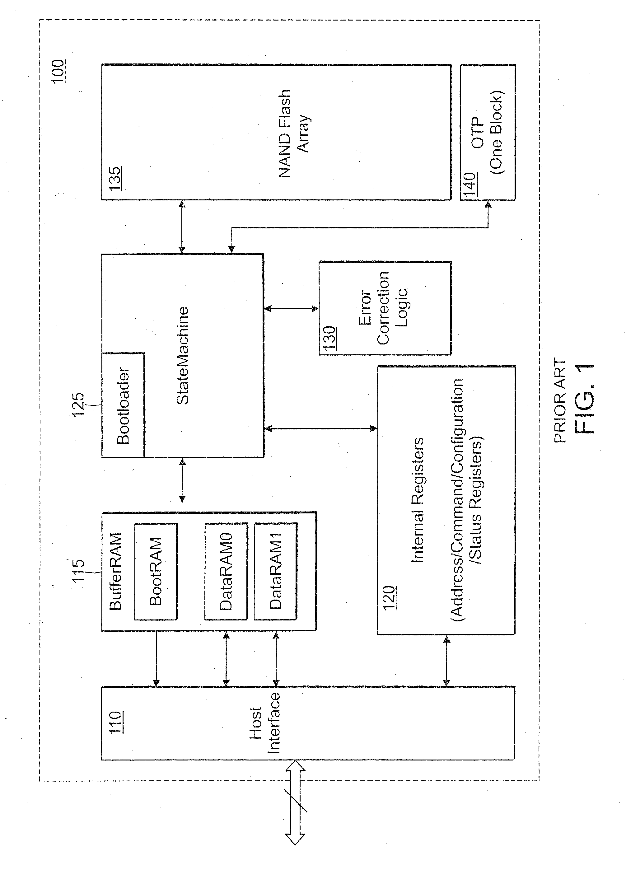
[0025]FIG. 1 illustrates an integrated Flash device 100 having a Flash memory 135 and control logic embedded in a single integrated circuit. The control logic includes a host interface 110 for communication with an external system, a memory buffer 115, a state machine 125 for interfacing with the memory 135, internal registers 120 and error correction logic 130. For example, during a read operation, the internal registers 120 receive commands and address data from the host interface 110. The state machine 125 receives this data and accesses the Flash memory 135 in accordance with the read operation. The state machine 125 receives sequential data from the Flash memory 135, from which it retrieves the requested data. After verification by error correction logic 130, the requested data is sent to memory buffer 115 for transmittal to the external system. Further details on the operation of a Flash memory device with an ...
PUM
Abstract
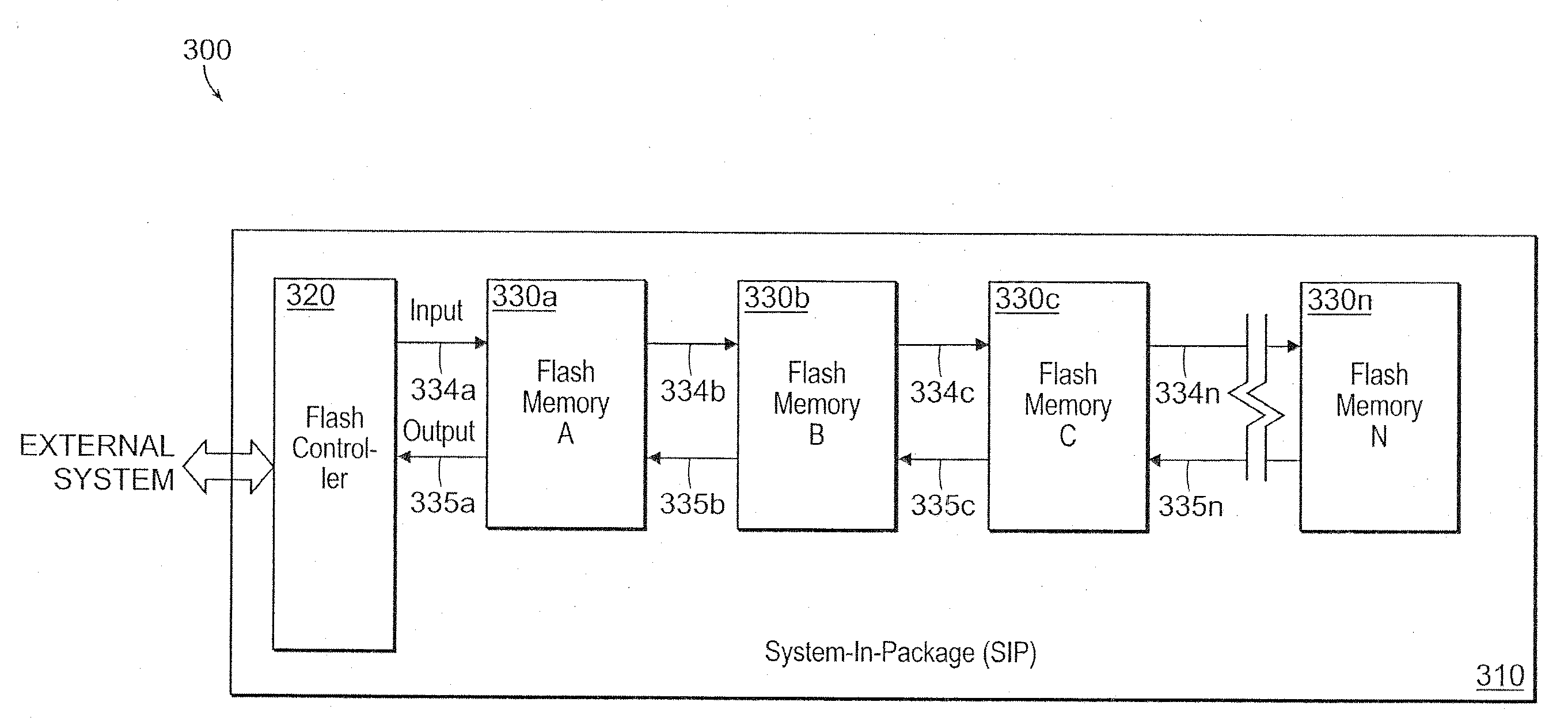
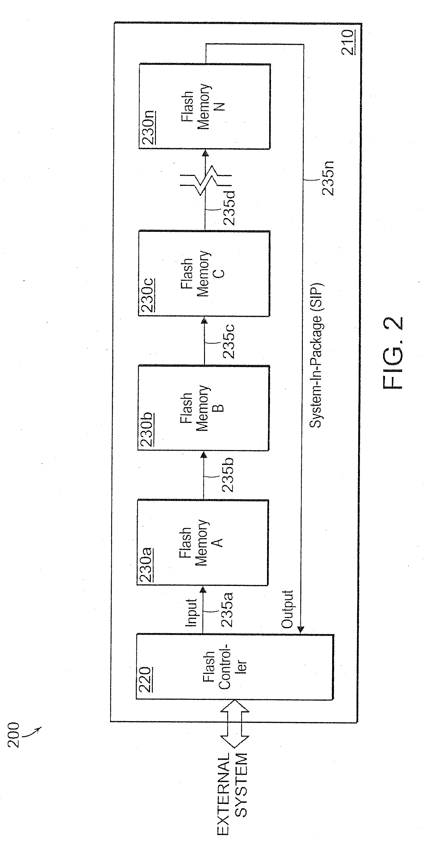
A Flash memory system is implemented in a system-in-package (SIP) enclosure, the system comprising a Flash memory controller and a plurality Flash memory devices. An SIP relates to a single package or module comprising a number of integrated circuits (chips). The Flash memory controller is configured to interface with an external system and a plurality of memory devices within the SIP. The memory devices are configured in a daisy chain cascade arrangement, controlled by the Flash memory controller through commands transmitted through the daisy chain cascade.
Description
RELATED APPLICATIONS[0001]This application is a continuation of U.S. application Ser. No. 11 / 639,375, filed on Dec. 14, 2006, claiming the benefit of U.S. Provisional Application No. 60 / 839,534, filed on Aug. 23, 2006, which is a continuation-in-part of U.S. application Ser. No. 11 / 496,278, filed on Jul. 31, 2006, which claims the benefit of U.S. Provisional Application No. 60 / 787,710, filed on Mar. 28, 2006, and which is a continuation-in-part of U.S. application Ser. No. 11 / 324,023, filed on Dec. 30, 2005, which claims the benefit of U.S. Provisional Application No. 60 / 722,368, filed on Sep. 30, 2005. The entire teachings of the above applications are incorporated herein by reference.BACKGROUND OF THE INVENTION[0002]Flash memory is a key enabling technology for consumer applications and mobile storage applications such as flash cards, digital audio & video players, cell phones, USB flash drivers and solid state disks for HDD replacement. As the demand increases for higher density ...
Claims
Application Information
Patent Timeline
Application Date:The date an application was filed.
Publication Date:The date a patent or application was officially published.
First Publication Date:The earliest publication date of a patent with the same application number.
Issue Date:Publication date of the patent grant document.
PCT Entry Date:The Entry date of PCT National Phase.
Estimated Expiry Date:The statutory expiry date of a patent right according to the Patent Law, and it is the longest term of protection that the patent right can achieve without the termination of the patent right due to other reasons(Term extension factor has been taken into account ).
Invalid Date:Actual expiry date is based on effective date or publication date of legal transaction data of invalid patent.
Patent Type & AuthorityApplications(United States)

