Lead frame package

a leadframe and package technology, applied in the direction of semiconductor devices, semiconductor/solid-state device details, electrical apparatus, etc., can solve the problems of poor signal integrity, limiting the speed of leadframe packages currently available to low frequency applications, and packages yet to meet the rate requirements of modern serdes systems

Active Publication Date: 2010-02-11
INTEGRATED DEVICE TECH INC
View PDF8 Cites 33 Cited by
  • Summary
  • Abstract
  • Description
  • Claims
  • Application Information

AI Technical Summary

Benefits of technology

[0008]Consistent with embodiments of the present invention, a lead frame package is disclosed that includes a first pair of lead frames configured to carry transmission signals and coupled to a first pair of die pads by a first pair of bond wires that are separated by less than three times the diameter of one of the first pair of bond wires. In some embodiments, a second pair of lead frames, the second pair of lead frames configured to carry a ground / power pair and coupled to a second pair of die pads that are adjacent to the first pair of die pads by a second pair of bond wires that are separated by less than three times the diameter of one of the second pair of bond wires, may also be included. In some embodiments, the transmission signals are serial receive or transmit differential signals.

Problems solved by technology

The higher impedance inputs due to high capacitive and inductive coupling between bonding wires can lead to restrictions on the speed of such packages.
Poor signal integrity restricts currently available leadframe packages to low frequency applications.
However, these packages are yet unable to meet the rate requirements of modern SerDes systems.

Method used


Image

  • Lead frame package
  • Lead frame package
  • Lead frame package

Examples


Embodiment Construction

[0025]In the following description specific details are set forth describing certain embodiments of the invention. It will be apparent, however, to one skilled in the art that the present invention may be practiced without some or all of these specific details. The specific embodiments presented are meant to be illustrative of the present invention, but not limiting. One skilled in the art may realize other material that, although not specifically described herein, is within the scope and spirit of this disclosure.

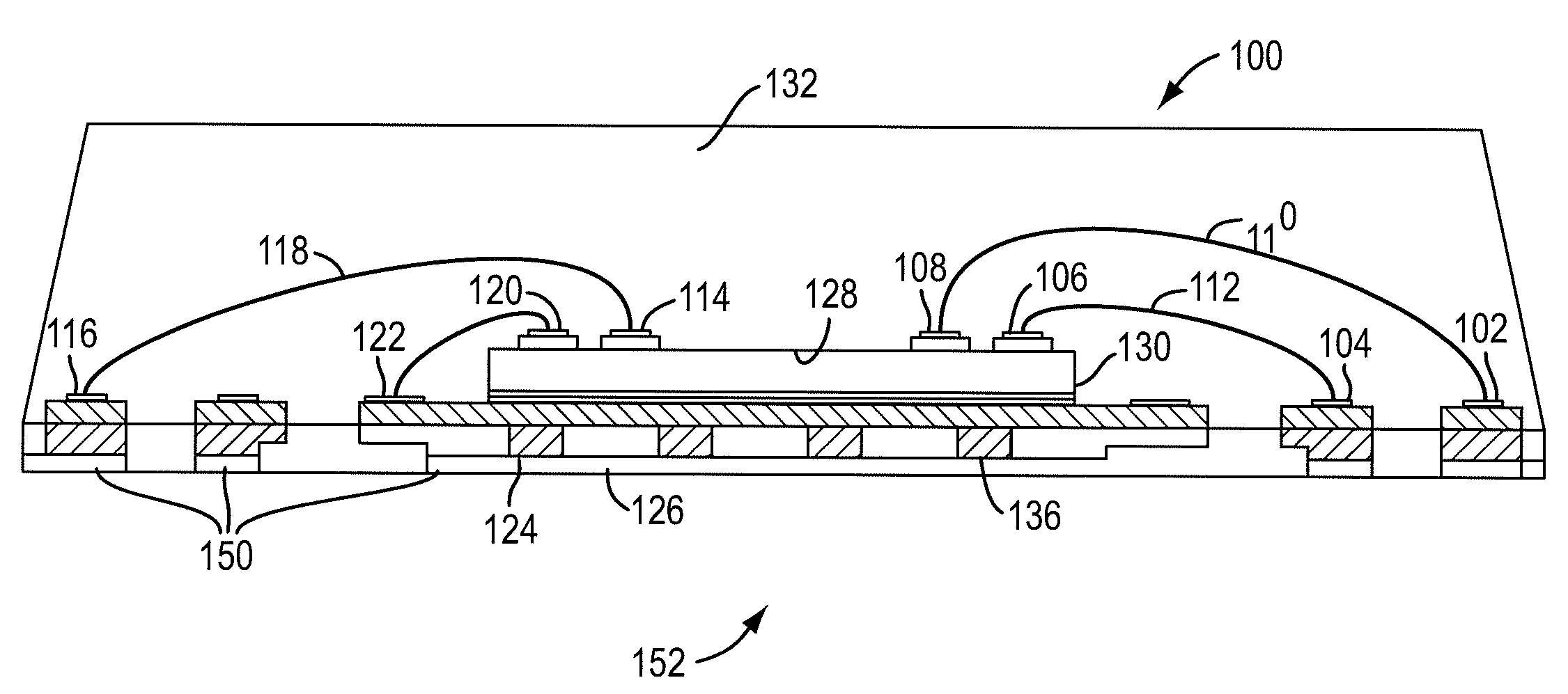
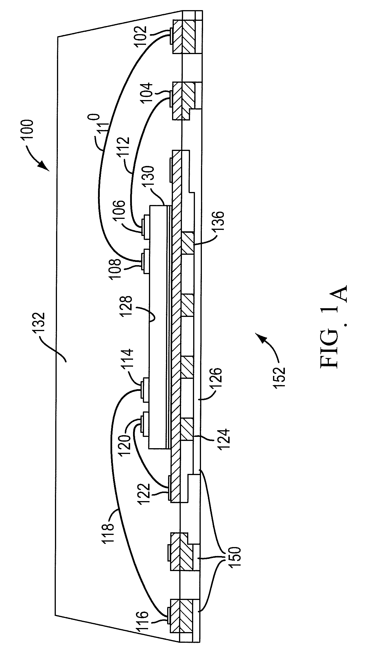
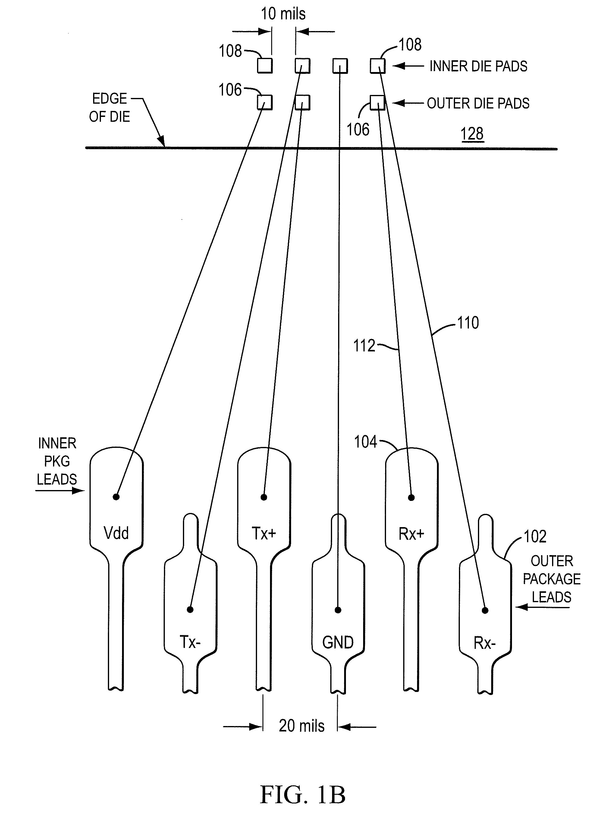
[0026]Some embodiments of the invention provide an improved lead frame package to allow serial data transfer rates in excess of 2 Gbits / sec. These rates can be accomplished by establishing sequences of high speed signal pairs with proximity placement, one to another, approximating a system line impedance (e.g. 50 ohms). In some embodiments, differential power / ground pairs positioned between high speed pairs can provide isolation to minimize crosstalk between signal pairs. ...


PUM


Abstract

A lead frame package is disclosed where transmission signals are coupled into a die from a pair of lead frames through bonding wires that are separated by no more than three times a diameter of one of the bonding wires. In some embodiments, pairs of lead frames carrying differential transmission signals can be shielded by adjacent pairs of ground and power leads that are coupled into the die through bonding wires that are also separated by no more than three times a diameter of one of the bonding wires.

Description

BACKGROUND[0001]1. Technical Field[0002]The present invention is related to a lead frame package and, in particular, a lead frame package that can be utilized for high performance serializer / deserializer (SerDes) applications.[0003]2. Discussion of Related Art[0004]Recently available small dimension lead frame packages offer significant cost savings advantages. Heat dissipation in these packages is improved with the die mounted about an exposed die pad. Staggered leads increase lead count and reduce package size. Reduced package height improves signal integrity with leads soldered directly to a top layer of a printed board metallization.[0005]The speed with which signals can be inserted into a die in the lead-frame package is dependent on multiple factors. Those parameters include the inductance of wire bonds, the capacitance of the wire bonds, and the resistance of the wirebonds. The higher impedance inputs due to high capacitive and inductive coupling between bonding wires can lea...

Claims


Application Information

Patent Timeline
Patent Type & Authority Applications(United States)
IPC IPC(8): H01L23/495H01L21/00
CPCH01L23/49503H01L2224/48644H01L23/49822H01L24/06H01L24/45H01L24/49H01L2224/05553H01L2224/05599H01L2224/05644H01L2224/45144H01L2224/48091H01L2224/48247H01L2224/48257H01L2224/49171H01L2224/49433H01L2224/73265H01L2224/85399H01L2924/01005H01L2924/01079H01L2924/01082H01L2924/014H01L2924/19041H01L2924/30105H01L2924/30107H01L2924/3011H01L2924/3025H01L23/49541H01L2924/00014H01L2924/01033H01L2924/01023H01L2924/01006H01L2224/32245H01L24/48H01L2924/00H01L2924/00012H01L2224/45015H01L2924/181H01L2224/05554H01L24/73H01L2924/20752
Inventor PILLING, DAVID J.SHAH, JITESHPENG, DIANEHUANG, DEREK
Owner INTEGRATED DEVICE TECH INC
Why Eureka
Try Eureka