Flash memory storage system and data writing method thereof

Active Publication Date: 2010-02-18
PHISON ELECTRONICS
View PDF2 Cites 106 Cited by
  • Summary
  • Abstract
  • Description
  • Claims
  • Application Information

AI Technical Summary

Benefits of technology

[0008]Accordingly, the present invention is directed to a flash memory storage system, which can effectively shorten a response time required when a host system sends a flush command t

Problems solved by technology

However, with progress of a fabrication process of the flash memory, while a volume design of each physical block becomes greater, time spent on moving the aforementioned old valid data is comparatively increased, so that when the host executes the write command, a relatively long response time has to be waited.
Particularly, when the flash memory storage system (for example, the SSD) applying a multi level cell (MLC) NAND flash memory as a storage medium is used as a main hard disk for a host system, the relative

Method used


Image

  • Flash memory storage system and data writing method thereof
  • Flash memory storage system and data writing method thereof
  • Flash memory storage system and data writing method thereof

Examples


first exemplary embodiment

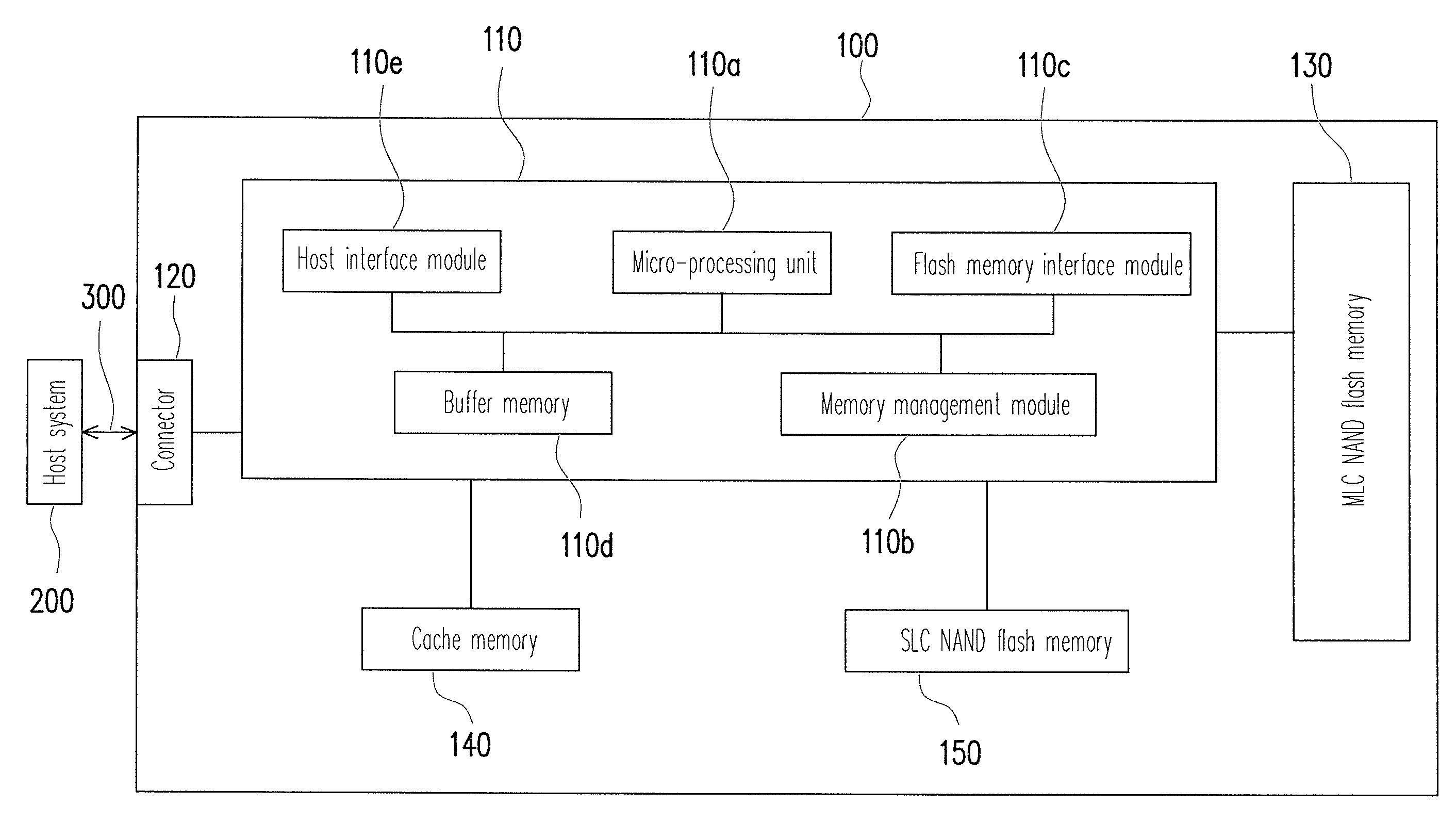
[0026]FIG. 1 is a schematic block diagram illustrating a flash memory storage system according to a first exemplary embodiment of the present invention. Referring to FIG. 1, the flash memory storage system 100 includes a controller 110, a connector 120, a MLC NAND flash memory 130, a cache memory 140 and a SLC NAND flash memory 150.

[0027]Generally, the flash memory storage system 100 is utilized together with a host system 200, so that the host system 200 can write data into the flash memory storage system 100 or read data from the flash memory storage system 100. In the present exemplary embodiment, the flash memory storage system 100 is a solid state drive (SSD) and is applied in the host system 200 to serve as a main hard disk. It should be understood that in another exemplary embodiment, the flash memory storage system 100 can also be a memory card or a flash drive.

[0028]The controller 110 can execute a plurality of commands implemented by hardware, firmware or software to perfo...

second exemplary embodiment

[0059]FIG. 5 is a schematic block diagram illustrating a flash memory storage system according to a second exemplary embodiment of the present invention. Referring to FIG. 5, the flash memory storage system 400 includes a controller 410, a connector 420, a MLC NAND flash memory 430 and a cache memory 440, and the flash memory storage system 400 is a SSD.

[0060]Hardware structures of the controller 410, the connector 420 and the cache memory 440 are the same to that of the controller 110, the connector 120 and the cache memory 140 of the first exemplary embodiment, and detailed description thereof is not repeated.

[0061]It should be noted that the flash memory storage system 400 has a different hardware configuration compared to that of the flash memory storage system 100, so that the memory management module 410b of the controller 410 has the machine commands for executing the data writing steps (shown as FIG. 6) of the present exemplary embodiment. Besides, a micro-processing unit 41...


PUM


Abstract

A flash memory storage system and a data writing method thereof are provided. The flash memory storage system includes a controller, a connector, a cache memory, a SLC NAND flash memory and a MLC NAND flash memory. When the controller receives data to be written into the MLC NAND flash memory from a host system, the data is temporarily stored in the cache memory first and then is written into the MLC NAND flash memory from the cache memory. And, the controller may backup the data stored in the cache memory to the SLC NAND flash memory. Accordingly, it is possible to reduce a response time for a flush command, thereby improving a performance of the flash memory storage system.

Description

CROSS-REFERENCE TO RELATED APPLICATION[0001]This application claims the priority benefit of Taiwan application serial no. 97130697, filed on Aug. 12, 2008. The entirety of the above-mentioned patent application is hereby incorporated by reference herein and made a part of specification.BACKGROUND[0002]1. Technology Field[0003]The present invention relates to a storage system. More particularly, the present invention relates to a flash memory storage system applying a multi level cell (MLC) NAND flash memory as a storage medium, and a data writing method thereof.[0004]2. Description of Related Art[0005]With a quick developing of digital camera, cell phone camera and MP3, demand of storage media by customers is increased greatly. Since a flash memory has the advantages of non-volatile, energy saving, small size and none mechanical structure etc., it is suitable for portable applications, and especially for portable battery-powered products. For example, a solid state disk (SSD) is a s...

Claims


Application Information

Patent Timeline
IPC IPC(8): G06F12/00
CPCG06F12/0804G06F2212/214G06F2212/1024G06F12/0868
Inventor YEH, CHIH-KANG
Owner PHISON ELECTRONICS
Why Eureka
Try Eureka