Printed circuit board and method of manufacturing the same

a printed circuit board and manufacturing method technology, applied in the direction of printed circuit manufacturing, printed circuit aspects, semiconductor/solid-state device details, etc., can solve the problems of reducing the coupling force between two metals, reducing the reliability of bump bonding, and limiting the coping of flip-chip packaging, so as to enhance contact reliability

Inactive Publication Date: 2010-02-25
SAMSUNG ELECTRO MECHANICS CO LTD
View PDF7 Cites 22 Cited by
  • Summary
  • Abstract
  • Description
  • Claims
  • Application Information

AI Technical Summary

Benefits of technology

[0012]An advantage of the present invention is that it provides a PCB in which a surface-treatment layer is provided between a post and a bump, thereby enhancing contact reliability between the post and the bump, and a method of manufacturing the same.
[0013]Additional aspect and advantages of the present general inventive concept will be set forth in part in the description which follows and, in part, will be obvious from the description, or may be learned by practice of the general inventive concept.
[0014]According to an aspect of the invention, a PCB comprises a substrate having a pad; a solder resist disposed on the substrate and exposing the pad; a post disposed on the post; a surface-treatment layer disposed on the post; and a bump disposed on the surface-treatment layer.
[0016]The PCB may further comprise an interface layer disposed between the pad and the post.
[0017]The bump may be formed on a top surface of the post, the bump having a cap shape.

Problems solved by technology

However, the flip-chip packaging has a limit in coping with such a technical trend that a circuit pattern and a pad of the PCB are gradually miniaturized.
The excessive stress may destroy the bump, and thus the bonding reliability of the bump may be degraded.
However, when the thickness of the inter-metallic compound excessively increases, the coupling force between two metals decreases.
In particular, when the metal post form of Cu is directly contacted with the solder, it is much more difficult to control the thickness of the inter-metallic compound.
The oxidization of the metal post may degrade the wettability of the solder for the post.
Therefore, although the bump with a minute pitch can be formed by providing the metal post on the package substrate for the flip-chip packaging, the contact reliability between the post and the bump is degraded due to the inter-metallic compound and the oxidization of the post.

Method used


Image

  • Printed circuit board and method of manufacturing the same
  • Printed circuit board and method of manufacturing the same
  • Printed circuit board and method of manufacturing the same

Examples


Embodiment Construction

[0030]Reference will now be made in detail to the embodiments of the present general inventive concept, examples of which are illustrated in the accompanying drawings, wherein like reference numerals refer to like elements throughout. The embodiments are described below in order to explain the present general inventive concept by referring to the figures. In the drawings, the thicknesses of layers and regions are exaggerated for clarity.

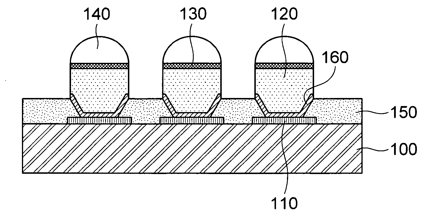
[0031]FIG. 1 is a cross-sectional view of a PCB according to an embodiment of the present invention.

[0032]Referring to FIG. 1, a pad 110 is disposed on a substrate 100. The substrate 100 may be a semiconductor substrate or circuit board, and is not limited thereto. For example, the substrate 100 may be a multi-layer circuit board including circuit layers and insulating layers which are alternately laminated.

[0033]The substrate 100 is electrically connected through the pad to an external part, for example, a semiconductor chip. Although not shown, a c...


PUM

PropertyMeasurementUnit
inter-metallicaaaaaaaaaa
shapeaaaaaaaaaa
sizeaaaaaaaaaa

Abstract

Provided is a printed circuit board (PCB) including a substrate that has a pad formed thereon; solder resist that is disposed on the substrate so as to expose the pad; a post that is disposed on the post; a surface-treatment layer that is disposed on the post; and a bump that is disposed on the surface-treatment layer.

Description

CROSS-REFERENCE TO RELATED APPLICATIONS[0001]This application claims the benefit of Korean Patent Application No. 10-2008-0080986 filed with the Korean Intellectual Property Office on Aug. 19, 2008, the disclosure of which is incorporated herein by reference.BACKGROUND OF THE INVENTION[0002]1. Field of the Invention[0003]The present invention relates to a printed circuit board (PCB) and a method of manufacturing the same.[0004]2. Description of the Related Art[0005]Recently, as electronic products are reduced in size and weight, semiconductor parts provided in the electronic products have been reduced in size and weight. To cope with such a technical trend, an interest in a packaging technique for mounting semiconductor elements on a PCB for package is increasing.[0006]Among a plurality of packaging techniques, flip-chip packaging is to directly connect a conductive pad of a semiconductor chip to a conductive pad of a PCB through a conductive solder bump. Accordingly, since the flip...

Claims


Application Information

Patent Timeline
Patent Type & Authority Applications(United States)
IPC IPC(8): H05K1/11H05K1/09H05K3/00
CPCH01L21/4853H01L23/49816H05K3/243H05K3/244H05K3/3473Y10T29/49149H05K2201/0367H05K2203/025H05K2203/043H05K2203/054H01L2224/16H05K3/4007H01L2224/05001H01L2224/05022H01L2224/05026H01L2224/05027H01L2224/05111H01L2224/05144H01L2224/05147H01L2224/05155H01L2224/05164H01L2224/05568H01L2224/05644H01L2224/05655H01L2224/05664H01L2924/00014H01L2924/01079H01L2924/013H01L2924/01028H05K1/02
Inventor LEE, DONG GYUMUN, SEON JAECHOI, JIN WONCHUNG, TAE JOON
Owner SAMSUNG ELECTRO MECHANICS CO LTD
Why Eureka
Try Eureka