Printed wiring board and method for manufacturing the same

a printing board and wiring board technology, applied in the direction of printed circuit, non-conductive material with dispersed conductive material, conductive pattern formation, etc., can solve the problems of insulation deterioration, hardly being used as means for electrically connecting a metallic substrate and a conductive layer in the printed wiring board for a magnetic head suspension, etc., to achieve the effect of effectively destroying and removing the printed wiring board without reducing the productivity of the board

Active Publication Date: 2010-02-25
SUMITOMO ELECTRIC IND LTD +1
View PDF15 Cites 15 Cited by
  • Summary
  • Abstract
  • Description
  • Claims
  • Application Information

AI Technical Summary

Benefits of technology

[0028]In the method for manufacturing a printed board, it is preferable that the period during which the current is applied be 1×10⁻⁶ seconds to 100 seconds. In this configuration,

Problems solved by technology

Although the above described conductive paste is effective as means for electrically connecting conductive layers made of copper foils to each other, it can hardly be used as means for electri

Method used


Image

  • Printed wiring board and method for manufacturing the same
  • Printed wiring board and method for manufacturing the same
  • Printed wiring board and method for manufacturing the same

Examples


example 1

[0086]In the fabricated printed wiring board 30, current of 1 A (that is, a current density of 8.0 A / mm2) was applied for one second to the interface between the metallic substrate 2 and the conductive paste 7, and the resistance of the metallic substrate 2 and the conductive paste 7 at the through hole 6a (hereinafter, referred to as resistance after current application) was measured, and the contact resistance of the metallic substrate 2 and the conductive paste 7 at the through hole 6a (hereinafter, referred to as contact resistance after current application) was measured by four-terminal sensing. The results are shown in Table 1.

example 2

[0087]In the fabricated printed wiring board 30, current of 2 A (that is, a current density of 15.9 A / mm2) was applied for one second to the interface between the metallic substrate 2 and the conductive paste 7, and the resistance of the metallic substrate 2 and the conductive paste 7 at the through hole 6a after the current application and the contact resistance after the current application were measured by four-terminal sensing. The results are shown in Table 1.

example 3

[0088]In the fabricated printed wiring board 30, current of 2 A (that is, a current density of 23.9 A / mm2) was applied for one second to the interface between the metallic substrate 3 and the conductive paste 7, and the resistance of the metallic substrate 2 and the conductive paste 7 at the through hole 6a after the current application and the contact resistance after the current application were measured by four-terminal sensing. The results are shown in Table 1.


PUM

PropertyMeasurementUnit
Timeaaaaaaaaaa
Timeaaaaaaaaaa
Lengthaaaaaaaaaa

Abstract

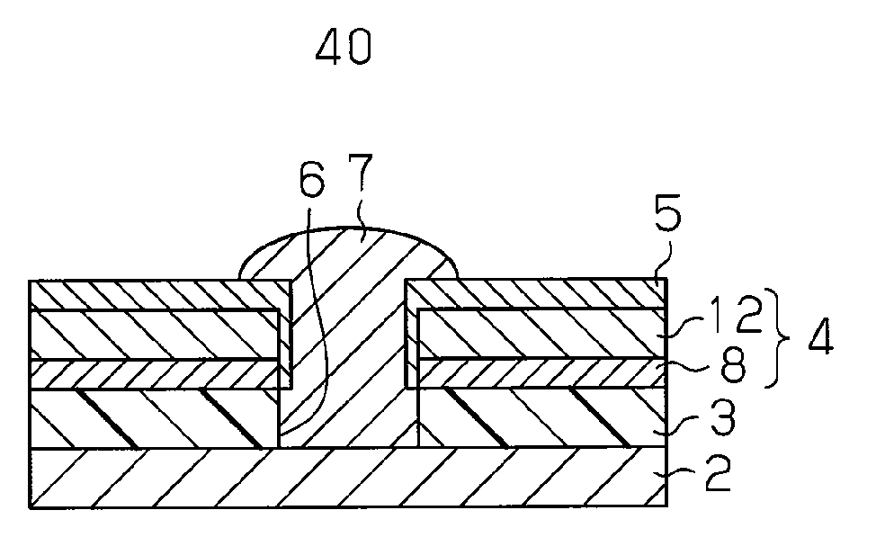
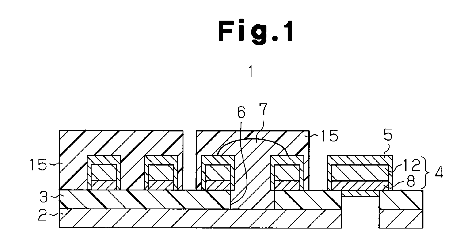
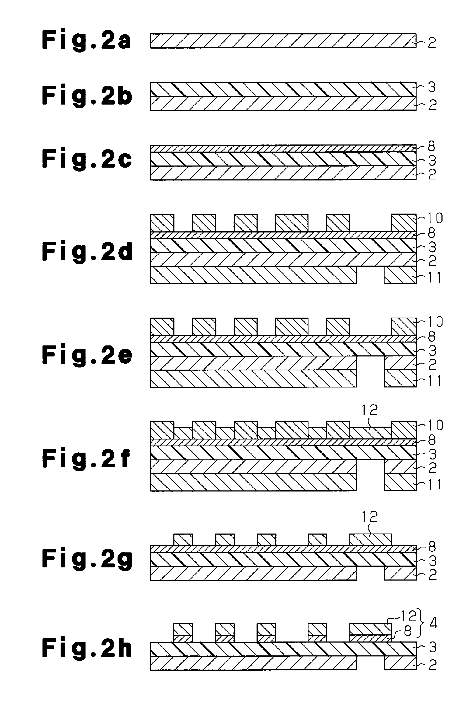
The printed wiring board 1 includes the metallic substrate 2, the insulating layer 3 provided on the surface of the metallic substrate 2, and the conductive layer 4 formed on the surface of the insulating layer 3. The conductive layer 4 is electrically connected to the metallic substrate 2. A bottomed via hole or a through hole 6 is formed in the insulating layer 3 and the conducive layer 4. The via hole has a bottom in the metallic substrate 2, and has a wall surface in the insulating layer 3 and in the conductive layer 4. The through hole 6 extends through the insulating layer 3, the conductive layer 4, and the metallic substrate 2. Conductive paste 7 fills the bottomed via hole or the through hole 6 to electrically connect the metallic substrate 2 and the conductive layer 4 with each other. The printed wiring board 1 is subjected to a process in which current is applied to the interface between the metallic substrate 2 and the conductive paste 7.

Description

FIELD OF THE INVENTION[0001]The present invention relates to a printed wiring board used as a substrate for a magnetic head suspension in a hard disk drive, and to a method for manufacturing the printed wiring board.BACKGROUND OF THE INVENTION[0002]In recent years, as the density of electronic devices is increased and as the sizes electronic devices are reduced, printed wiring boards have been applied to a variety of uses. For example, in a hard disk drive, in which high-speed transfer of data is required, a printed wiring board is used as a substrate for a magnetic head suspension on which a magnetic head is mounted.[0003]Patent Document 1 discloses such a printed wiring board having an insulating layer in which through hole is formed, conductive paste filling the through hole, and a conductive layer formed on either side of the insulating layer. Each conductive layer is formed of copper foil and has a predetermined wiring pattern. Since conductive paste generally has good conducti...

Claims


Application Information

Patent Timeline
IPC IPC(8): H05K1/11H05K3/10
CPCH05K1/056H05K3/4069H05K3/44H05K2201/09554H05K2203/0315Y10T29/49165H05K2203/1136H01B1/22H05K1/097Y10T29/49128H05K2203/105
Inventor OKA, YOSHIOPARK, JINJOOMAEDA, KAZUYUKIYAGI, NARITOSHIMOMURA, TETSUYANISHIKAWA, JUNICHIRO
Owner SUMITOMO ELECTRIC IND LTD
Why Eureka
Try Eureka