Organic light emitting display apparatus and method of manufacturing organic light emitting display apparatus

Active Publication Date: 2010-02-25
SAMSUNG DISPLAY CO LTD
View PDF2 Cites 69 Cited by
  • Summary
  • Abstract
  • Description
  • Claims
  • Application Information

AI Technical Summary

Benefits of technology

[0009]Aspects of the present invention provide an organic light emitting display (OLED) apparatus t

Problems solved by technology

Thus, such photolithography methods are complicated time consuming and are difficult to control, which can result in the production of a large number of defects

Method used


Image

  • Organic light emitting display apparatus and method of manufacturing organic light emitting display apparatus
  • Organic light emitting display apparatus and method of manufacturing organic light emitting display apparatus
  • Organic light emitting display apparatus and method of manufacturing organic light emitting display apparatus

Examples


Example

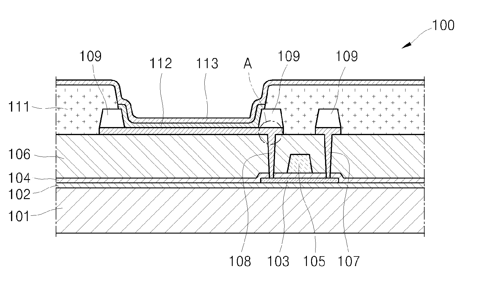
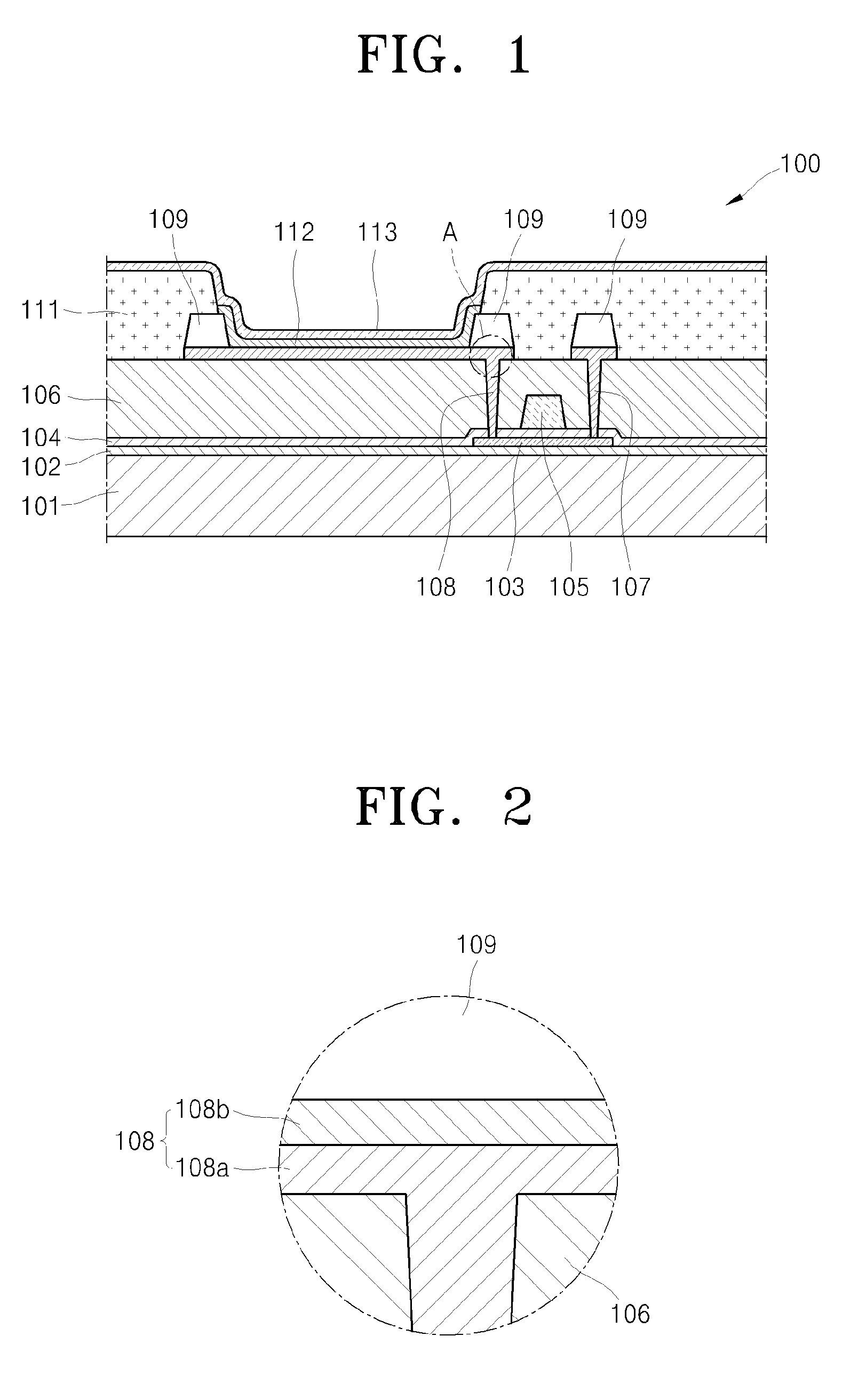
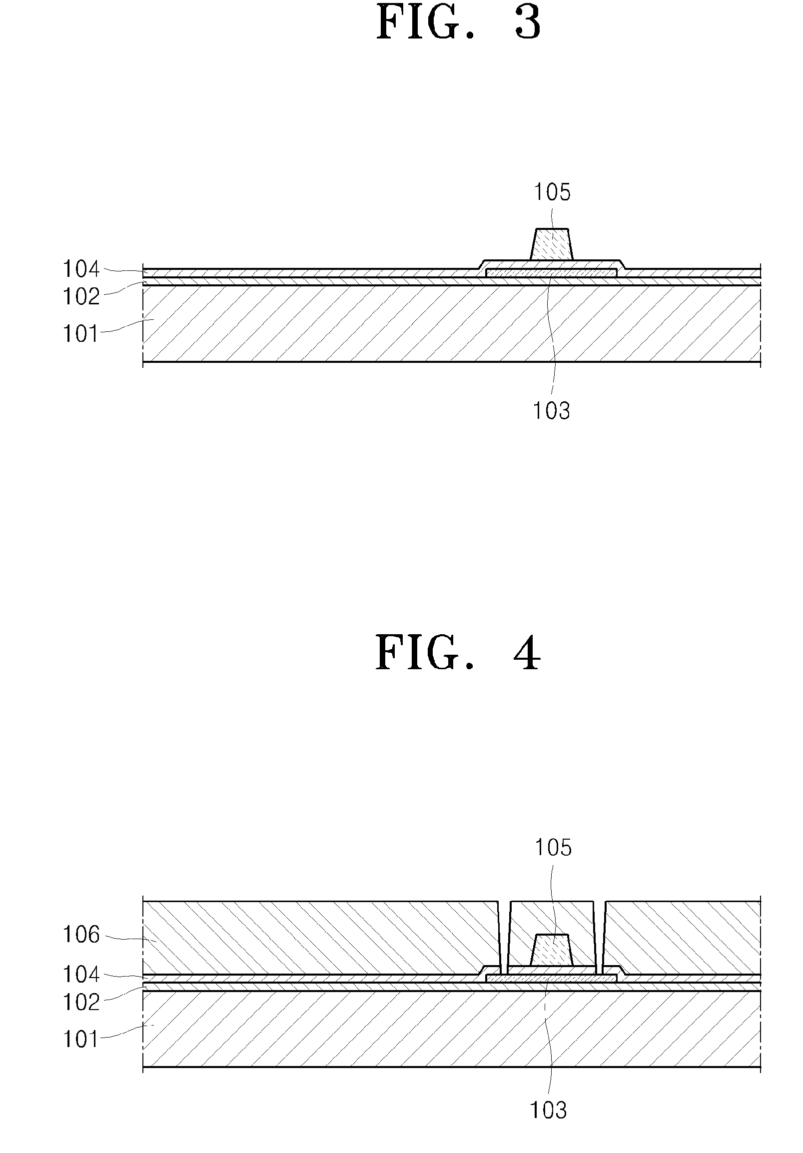
[0024]Reference will now be made in detail to the exemplary embodiments of the present invention, which are illustrated in the accompanying drawings, wherein like reference numerals refer to like elements throughout. The exemplary embodiments are described below, in order to explain the aspects of the present invention, by referring to the figures.

[0025]As referred to herein, when a first element is said to be disposed or formed “on”, or “adjacent to”, a second element, the first element can directly contact the second element, or can be separated from the second element by one or more other elements located therebetween. In contrast, when an element is referred to as being disposed or formed “directly on” another element, there are no intervening elements present. As used herein, the term “and / or” includes any and all combinations of one or more of the associated listed items.

[0026]FIG. 1 is a schematic cross-sectional diagram of an organic light emitting display (OLED) apparatus 1...


PUM


Abstract

An organic light emitting display (OLED) apparatus and a method of manufacturing the same, the OLED apparatus including: a substrate; an active layer formed on the substrate; a gate electrode insulated from the active layer; source and drain electrodes insulated from the gate electrode and electrically connected to the active layer; a pixel defining layer formed on the source and drain electrodes, having an aperture to expose one of the source and drain electrodes; an intermediate layer formed in the aperture and comprising an organic light emitting layer; and a facing electrode which is formed on the intermediate layer. One of the source and drain electrodes has an extension that operates as a pixel electrode. The aperture exposes the extended portion. The intermediate layer is formed on the extended portion.

Description

CROSS-REFERENCE TO RELATED APPLICATION[0001]This application claims the benefit of Korean Patent Application No. 2008-81069, filed on Aug. 19, 2008, in the Korean Intellectual Property Office, the disclosure of which is incorporated herein by reference.BACKGROUND OF THE INVENTION[0002]1. Field of the Invention[0003]Aspects of the present invention relate to an organic light emitting display (OLED) apparatus and a method of manufacturing the OLED apparatus.[0004]2. Description of the Related Art[0005]Many current electronic devices include a thin, flat-panel display apparatus. Such flat-panel display apparatuses can be classified as organic or inorganic light emitting display apparatuses, which are self-emitting display apparatuses that are regarded as next generation display apparatuses, due to having wide viewing angles, excellent contrast, and fast response speeds. Organic light-emitting display apparatuses, which include light emitting layers formed of an organic material to disp...

Claims


Application Information

Patent Timeline
IPC IPC(8): H01J1/63H01L21/00
CPCH01L27/3246H01L27/3248H01L27/3258H01L27/3265H01L27/3244H01L51/5218H01L51/56H01J9/261H01L51/5012H01L51/0018H10K59/122H10K59/123H10K59/124H10K59/1216H10K71/233H10K50/818H10K71/00H01L21/32115H10K59/12H10K50/11
Inventor KWON, DO-HYUNLEE, IL-JEONGIM, CHOONG-YOULNO, DAE-HYUNYU, CHEOL-HO
Owner SAMSUNG DISPLAY CO LTD
Why Eureka
Try Eureka