Multilayer Printed Wiring Board And Manufacturing Method For Same

Inactive Publication Date: 2008-05-29
PANASONIC CORP
View PDF8 Cites 20 Cited by
  • Summary
  • Abstract
  • Description
  • Claims
  • Application Information

AI Technical Summary

Benefits of technology

[0010]In the present invention, films having wires formed on both surfaces are pasted together using, for example, a woven cloth impregnated with a resin, as a prepreg, and therefore, wires can be prevented from short circuiting by the woven cloth included in the prepreg, even in a case where the films are pressed under high pressure. In addition, through holes are formed in the prepreg in advance and filled in with a

Problems solved by technology

At the time of this pasting, however, adhesive 14 is softened and becomes fluid

Method used


Image

  • Multilayer Printed Wiring Board And Manufacturing Method For Same
  • Multilayer Printed Wiring Board And Manufacturing Method For Same
  • Multilayer Printed Wiring Board And Manufacturing Method For Same

Examples


Example

First Embodiment

[0055]In the following, a multilayer board according to the first embodiment of the present invention is described in reference to the drawings.

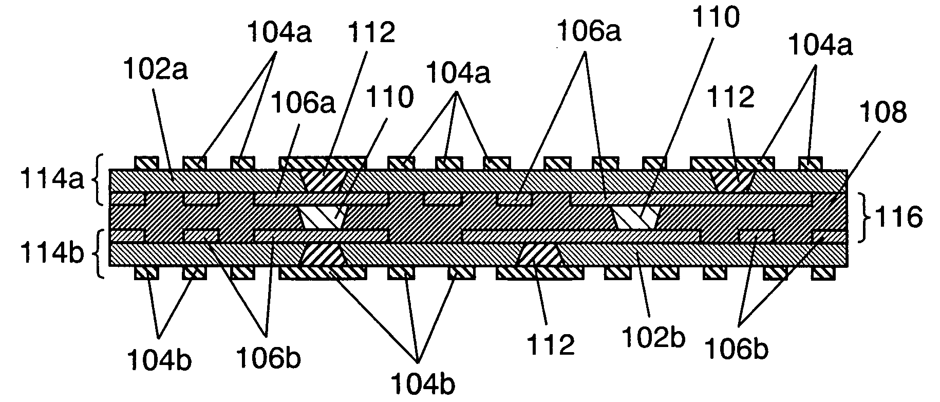
[0056]FIG. 1 is a cross sectional diagram showing a multilayer board according to the first embodiment of the present invention.

[0057]As shown in FIG. 1, the multilayer board has films 102a and 102b, first wires 104a and 104b, second wires 106a and 106b, insulating layer 108, IVH's 110, interlayer connection portions 112, two-sided boards 114a and 114b, and paste connection layer 116 as main components.

[0058]Here, first wires 104a are formed on one side of film 102a and second wires 106a are formed on the other side, and thus, two-sided board 114a is formed. Likewise, two-sided board 114b has first wires 104b and second wires 106b on the respective sides of film 102b, and the wires are connected to each other through interlayer connection portions 112. In addition, paste connection layer 116 is formed of insulating layer 108 ...

Example

Second Embodiment

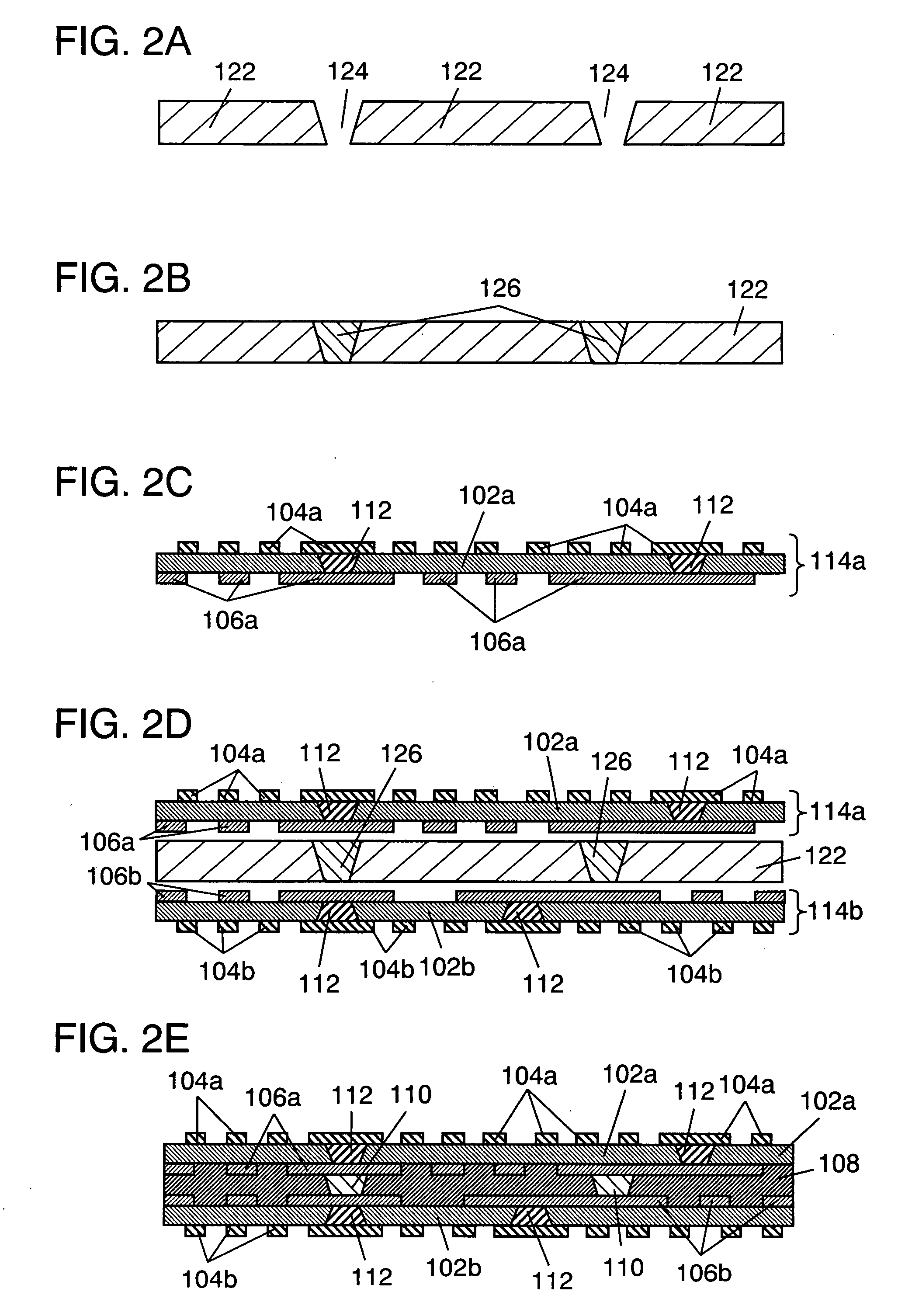
[0067]In the following, a manufacturing method for a multilayer board according to the second embodiment of the present invention is described. The second embodiment is an example of a manufacturing method for a four layer board, and corresponds to an example of a manufacturing method for the four layer board described in the first embodiment. FIGS. 2A to 2E are cross sectional diagrams showing a manufacturing method for a four layer board according to the second embodiment.

[0068]First, as shown in FIG. 2A, through holes 124 are formed in prepreg 122. At this time, it is desirable for through holes 124 to be formed in a state where the protective film is pasted on the surface of prepreg 122 in advance. A die, a drill, a laser or the like can be used to form through holes 124. Commercially available material, such as glass epoxy to be described below, an aramid epoxy or the like can be used as the material for the prepreg.

[0069]Next, as shown in FIG. 2B, through hole...

Example

Third Embodiment

[0086]In the following, the multilayer board according to the third embodiment of the present invention is described in reference to the drawings. The third embodiment is different from the first embodiment in the number of films used for multilayer (two in the first embodiment while three in the third embodiment).

[0087]FIG. 3 is a cross sectional diagram showing a multilayer board according to the third embodiment. FIG. 3 shows two-sided boards 114a, 114b and 114c made of films which are pasted together using two paste connection layers 116a and 116b. In addition, second wires 106a formed on the lower surface of two-sided board 114a are electrically connected to second wires 106b formed on the upper surface of two-sided board 114b through IVH's 110. In the same manner, second wires 106d formed on the upper surface of two-sided board 114c are electrically connected to second wires 106c formed on the lower surface of two-sided board 114b through IVH's 110.

[0088]In thi...


PUM

PropertyMeasurementUnit
Ratioaaaaaaaaaa
Electrical conductoraaaaaaaaaa
aaaaaaaaaa

Abstract

In a case of multilayer circuit boards where a plurality of conventional films are used as insulating layers, the films are connected with each other using an adhesive, and therefore, the adhesive sometimes negatively affects reduction in thickness. Therefore, a plurality of two-sided boards with films used therein are pasted together with a paste connection layer interposed therebetween, the paste connection layer being configured such that through holes formed in a prepreg are filled in with a conductive paste which is then cured, and second wires are electrically connected with each other through the conductive paste with which the through holes formed in the paste connection layer in advance are filled in, and thus, a multilayer board can be provided without using an adhesive, and the entirety of the multilayer circuit board can be reduced in thickness.

Description

TECHNICAL FIELD[0001]The present invention relates to a multilayer printed wiring board which is used for a cellular phone and an ultra-compact portable terminal, a multilayer printed wiring board which is used for an interposer used when a semiconductor chip is mounted as a bare chip, and a manufacturing method for the same.BACKGROUND ART[0002]Conventional multilayer printed wiring boards (hereinafter simply referred to as multilayer boards) of this type are known to be multilayer boards where IVH's (inner via holes) are formed at arbitrary positions. An example of such conventional multilayer boards is disclosed in, for example, Unexamined Japanese Patent Publication No. 2002-353619.[0003]However, further reduction in thickness of the layers of multilayer boards has been desired in the market. In the following, a multilayer board where films are used as a means for reducing the thickness of the layers of the multilayer board is described.[0004]FIG. 9 is a cross sectional diagram s...

Claims


Application Information

Patent Timeline
IPC IPC(8): H05K1/02H01R43/00
CPCH05K3/4069H05K3/4602H05K3/4614H05K3/462Y10T29/49117H05K3/4658H05K2201/10378H05K2203/061H05K3/4644H05K3/46
Inventor HIRAI, SHOGOECHIGO, FUMIONAKAMURA, TADASHISUGAWA, TOSHIO
Owner PANASONIC CORP
Why Eureka
Try Eureka