Optical reader
a technology of optical readers and optical slits, applied in the field of optical slits, can solve the problems of increased illumination light sources, increased space requirements, and devices of greater size and manufacturing costs
- Summary
- Abstract
- Description
- Claims
- Application Information
AI Technical Summary
Benefits of technology
Problems solved by technology
Method used
Image

Examples
Embodiment Construction
[0024]The present invention will now be described in detail based on the illustrated embodiments. The embodiments are described with reference to an optical reader capable of reading semiconductor wafer markings or defects.
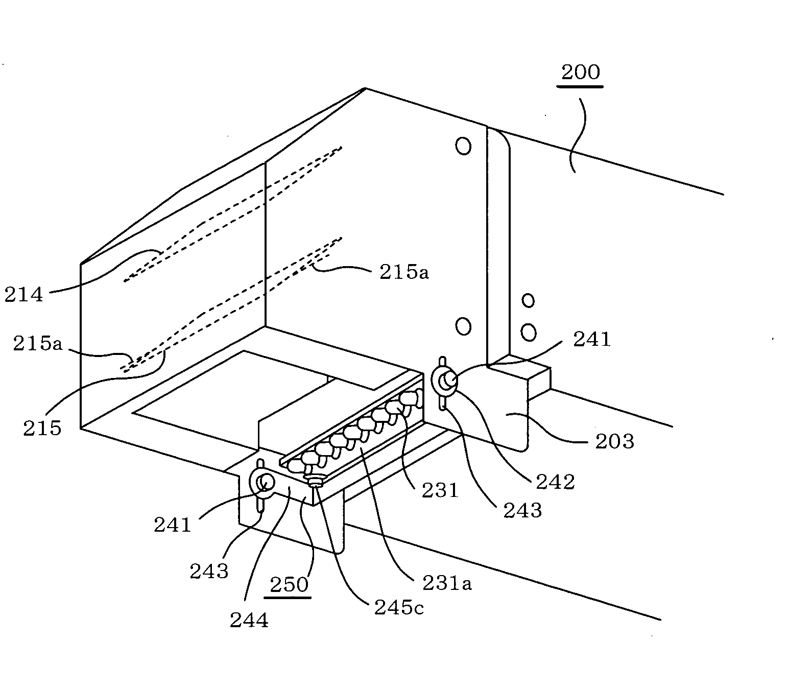
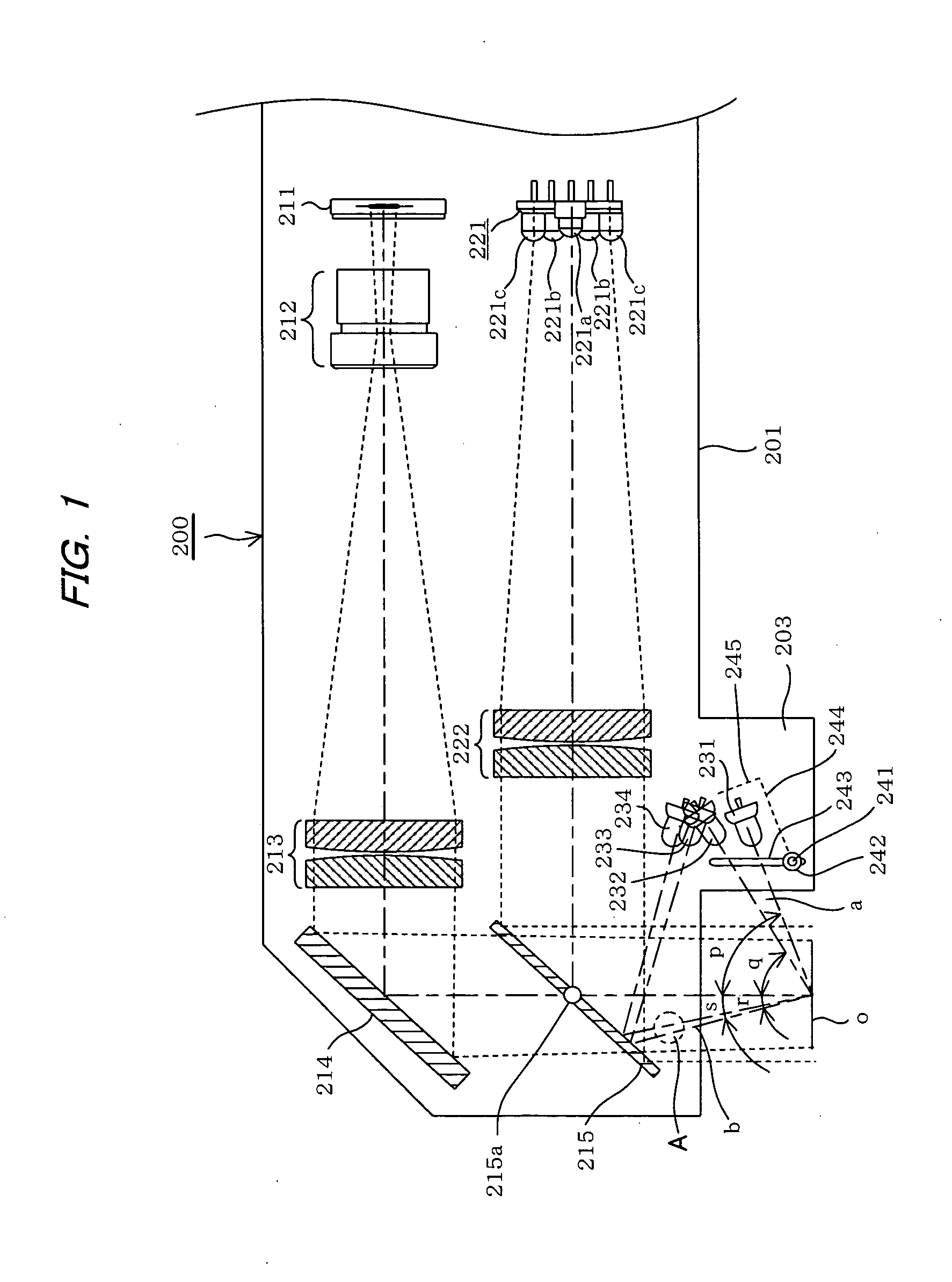
[0025]FIG. 1 shows the main structure of the photographing optical system and illumination optical system of an optical reader 200 according to the present invention. In FIG. 1, reference numeral 201 indicates the frame of the optical reader 200. The photographing optical system and illumination optical system are housed in the interior of the frame 201, which is composed of a plastic or metallic material, and is substantially L-shaped.
[0026]The photographing optical system includes an imaging device 211 that is composed of a CCD or CMOS sensor or the like, in front of which is disposed an optical system composed of a front lens assembly 213 and a rear lens assembly 212. A total reflection mirror 214 is disposed in front of the front lens assembly 213 to verticall...
PUM
 Abstract
Description
Claims
Application Information