Stacked-chip device

a technology of stacked chips and chips, applied in the direction of semiconductor devices, semiconductor/solid-state device details, electrical apparatus, etc., can solve the problems of increased production cost, performance decline, and inability to establish electrical connections

Inactive Publication Date: 2010-03-04
KK TOSHIBA
View PDF4 Cites 86 Cited by
  • Summary
  • Abstract
  • Description
  • Claims
  • Application Information

AI Technical Summary

Problems solved by technology

One of the problems with CoC is that electrical connections cannot be established by bumps alone when more than two chips are accommodated in a package, and performance decreases while production cost increases as the number of chips is increased.

Method used


Image

  • Stacked-chip device
  • Stacked-chip device
  • Stacked-chip device

Examples


embodiment

3. EMBODIMENT

(1) First Embodiment

[0046]FIG. 2 shows a through-silicon via according to a first embodiment of the invention.

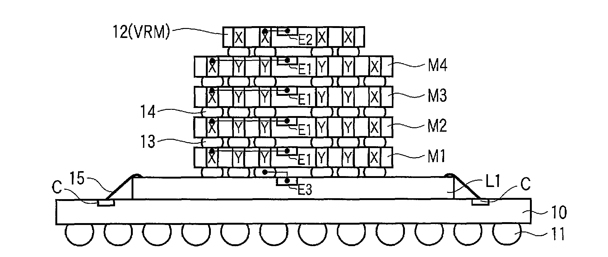
[0047]Chips L1, M1, M2, and 12 having different functions are mounted on the package board 10. For example, the BGA terminal 11 is disposed in the lower surface of the package board 10.

[0048]Chip L1 is the control chip (for example, CPU). Control chip L1 is connected to the conductive line C on the package board 10 through the bonding wire 15.

[0049]Chips M1 and M2 are the memory chip. Memory chip M1 is stacked on control chip L1, and memory chip M2 is stacked on memory chip M1.

[0050]Chip 12 is the VRM chip. The VRM chip 12 is stacked on memory chip M2.

[0051]The bumps 13 are disposed between control chip L1 and memory chip M1, between memory chip M1 and memory chip M2, and between memory chip M2 and the VRM chip 12.

[0052]Memory chips M1 and M2 are the through-silicon-via chip. Each of memory chips M1 and M2 includes the semiconductor substrate, semiconductor inte...

second embodiment

(2) Second Embodiment

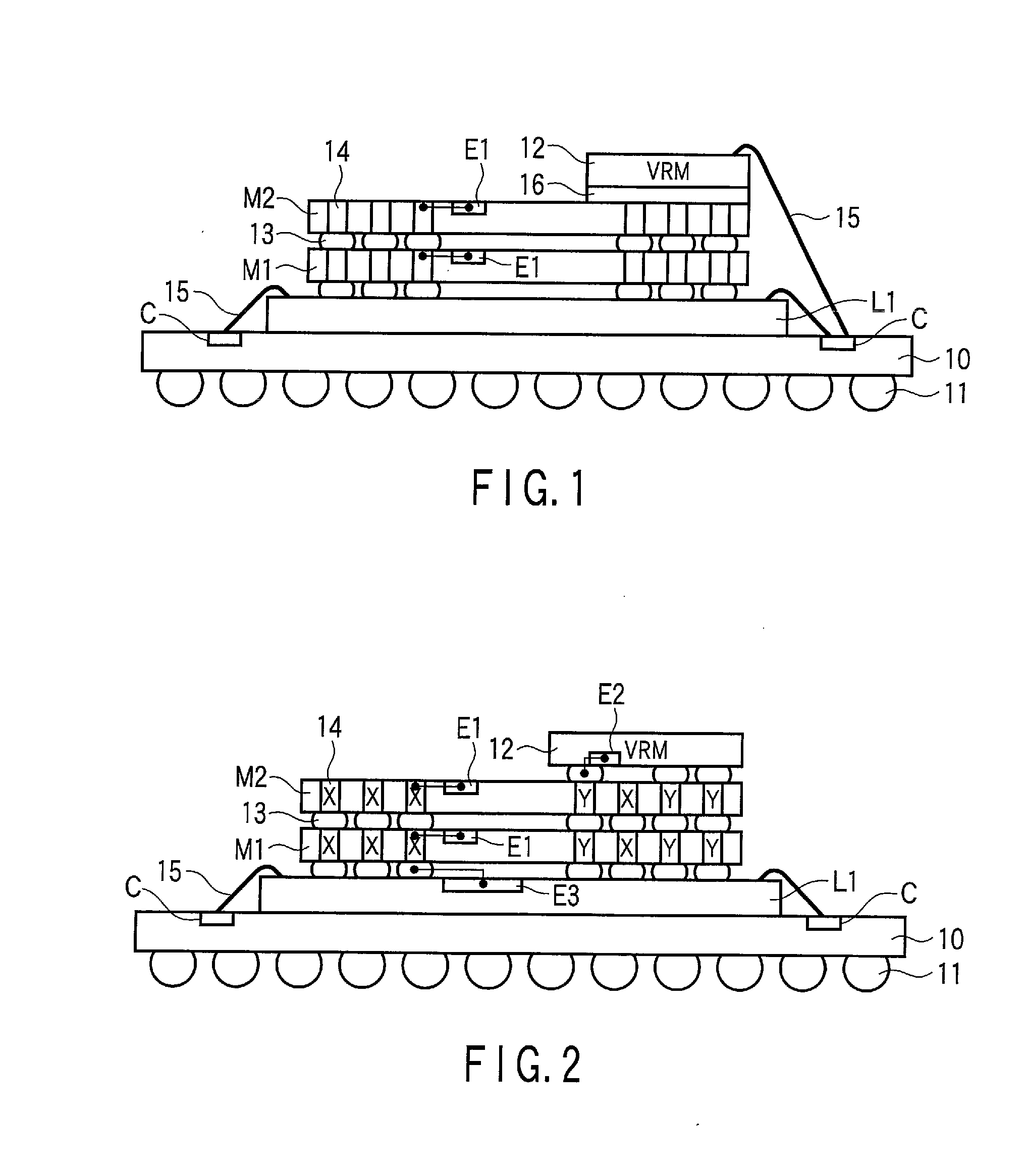
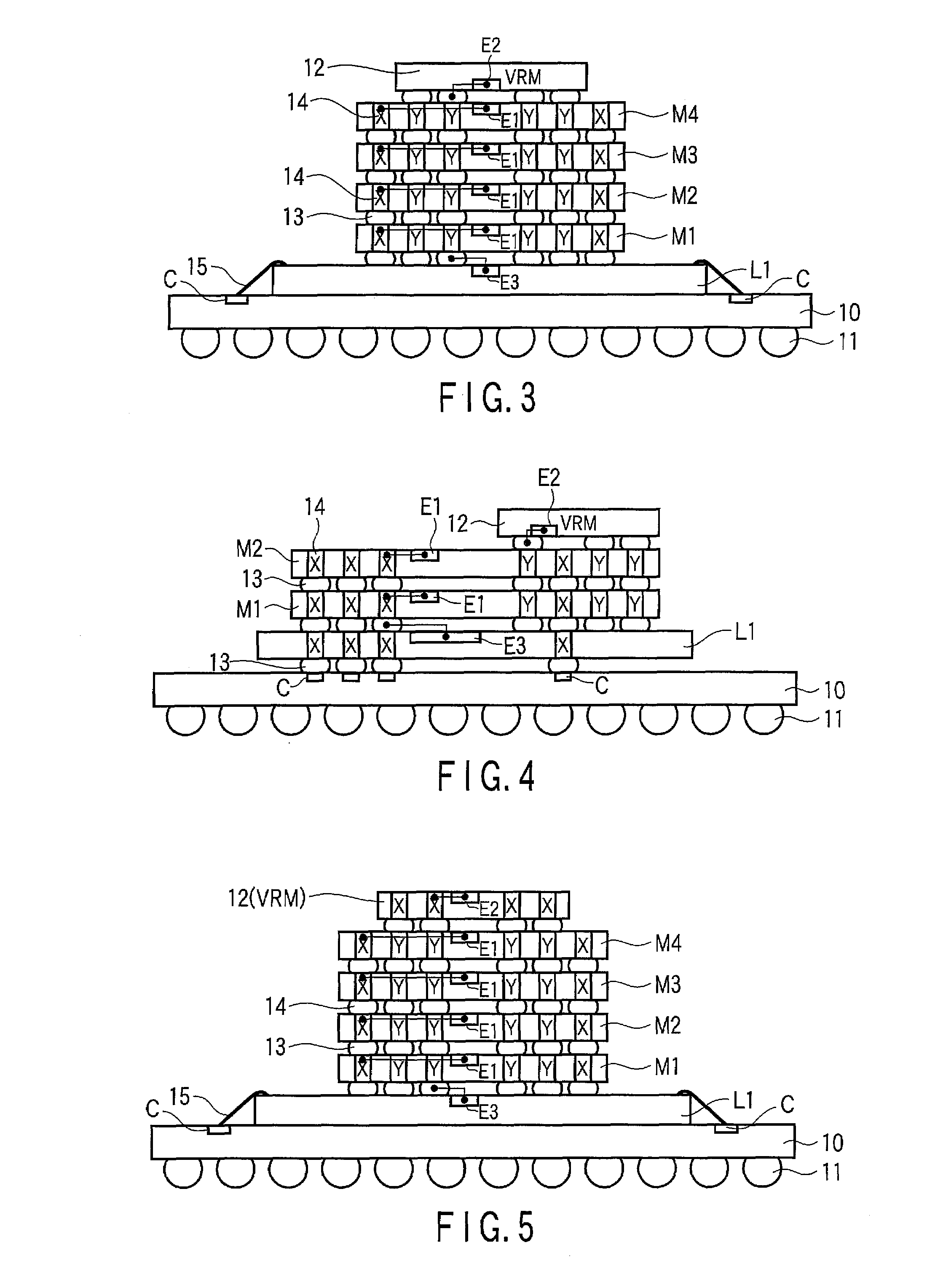
[0065]FIG. 3 shows a through-silicon via according to a second embodiment of the invention.

[0066]The second embodiment relates to an application example of the first embodiment.

[0067]TSV of the second embodiment differs from TSV of the first embodiment in the number of memory chips (M1 to M4) stacked on control chip L1 and the position of the VRM chip 12.

[0068]In TSV, there is no limitation to the number of memory chips stacked on control chip L1. In the second embodiment, four memory chips M1 to M4 are stacked on control chip L1. Preferably the number of memory chips stacked on control chip L1 is 2n (n is a natural number).

[0069]In the second embodiment, the VRM chip 12 is disposed in the centers of memory chips M1 to M4. The layouts of conductive layers 14(Y) that are the dummy through-silicon via in memory chips M1 to M4 are determined such that the VRM chip 12 can be disposed in the centers of memory chips M1 to M4.

third embodiment

(3) Third Embodiment

[0070]FIG. 4 shows a through-silicon via according to a third embodiment of the invention.

[0071]The third embodiment also relates to an application example of the first embodiment.

[0072]TSV of the third embodiment differs from TSV of the first embodiment in that control chip (for example, CPU) L1 is the through-silicon-via chip.

[0073]Control chip L1 includes the semiconductor substrate, semiconductor integrated circuit E3, and conductive layer 14(X). Semiconductor integrated circuit E3 is formed on one surface side of the semiconductor substrate. Conductive layer 14(X) is pierced from one surface side of the semiconductor substrate to the other surface side, and connected to semiconductor integrated circuit E3.

[0074]Semiconductor integrated circuit E3 in control chip L1 is connected to semiconductor integrated circuit E1 in each of memory chips M1 and M2 through conductive layer 14(X) in each of memory chips M1 and M2.

[0075]Semiconductor integrated circuit E3 in ...


PUM


Abstract

A stacked chip device includes a first chip having a first function, and a second chip having a second function which is different from the first function, which is stacked on the first chip. The first chip is a through-silicon-via chip which is comprised of a first semiconductor substrate having first and second surfaces, a first semiconductor integrated circuit which is provided on the first surface of the first semiconductor substrate, a first conductive layer connecting to the first semiconductor integrated circuit, which goes through the first surface of the first semiconductor substrate to the second surface of the first semiconductor substrate, and a second conductive layer not connecting to the first semiconductor integrated circuit, which goes through the first surface of the first semiconductor substrate to the second surface of the first semiconductor substrate. The first and second conductive layers have the same shape and the same structure.

Description

CROSS-REFERENCE TO RELATED APPLICATIONS[0001]This application is based upon and claims the benefit of priority from prior Japanese Patent Application No. 2008-216822, filed Aug. 26, 2008, the entire contents of which are incorporated herein by reference.BACKGROUND OF THE INVENTION[0002]1. Field of the Invention[0003]The present invention relates to a through-silicon via.[0004]2. Description of the Related Art[0005]A chip-on-chip (CoC) technique is well known as a technique of realizing miniaturization and speed enhancement of an LSI. In the CoC technique, chips having different functions are stacked and accommodated in a single package.[0006]In CoC, an electrical connection between the chips is established by a bump or a bonding wire. One of the problems with CoC is that electrical connections cannot be established by bumps alone when more than two chips are accommodated in a package, and performance decreases while production cost increases as the number of chips is increased.[0007...

Claims


Application Information

Patent Timeline
Patent Type & Authority Applications(United States)
IPC IPC(8): H01L23/48
CPCH01L23/481H01L2224/0401H01L24/16H01L24/32H01L24/48H01L24/73H01L25/0657H01L25/18H01L2224/32146H01L2224/48091H01L2224/48227H01L2224/73253H01L2224/73265H01L2225/06513H01L2225/06517H01L2225/06527H01L2225/06541H01L2924/14H01L2924/15311H01L23/49816H01L2924/10253H01L2224/16146H01L2224/13025H01L2224/05009H01L2224/14156H01L2224/14151H01L2924/00014H01L2924/00H01L2224/32145H01L2924/00012H01L2224/16145H01L2224/16227H01L2224/17181H01L2224/73207H01L2224/45099H01L2224/45015H01L2924/207
Inventor URAKAWA, YUKIHIRO
Owner KK TOSHIBA
Why Eureka
Try Eureka