Liquid crystal display panel and method for manufacturing the same

a liquid crystal display and liquid crystal technology, applied in liquid crystal compositions, instruments, chemistry apparatus and processes, etc., can solve the problems of mura or image sticking, lcd panel manufacturing still has image sticking problem, lcd panel using psa technology is susceptible to problems, etc., to achieve the effect of reducing the number of photosensitive monomers in liquid crystal material and improving the problem of image sticking

Active Publication Date: 2010-03-04
AU OPTRONICS CORP
View PDF5 Cites 34 Cited by
  • Summary
  • Abstract
  • Description
  • Claims
  • Application Information

AI Technical Summary

Benefits of technology

[0008]The invention is directed to a liquid crystal display (LCD) panel and a method for manufacturing the same. According to the invention, two processes of polymerization reaction are applied, the ultra-violet used in the second polymerization reaction has a larger wavelength, and at least one photosensitive monomer whose absorption peak is larger than 300 nm is added to the liquid crystal material which is used for absorbing the ultra-violet in the second polymerization reaction. Thus, the residual photosensitive monomers in the liquid crystal material are reduced, and the problem of image sticking can be improved.

Problems solved by technology

However, the LCD panel using PSA technology is susceptible to the problems such as Mura or image sticking.
Mura refers to the problem which occurs when local image has low contrast or non-uniformed luminance.
Image sticking refers to the problem which occurs if previous image stays for a long duration of time and is overlapped with the subsequent image when an image displayed on the LCD panel displays over a long duration is switched to another image.
However, despite the light initiator is added during the manufacturing process, the manufactured LCD panel still has image sticking problem.

Method used


Image

  • Liquid crystal display panel and method for manufacturing the same
  • Liquid crystal display panel and method for manufacturing the same
  • Liquid crystal display panel and method for manufacturing the same

Examples


Embodiment Construction

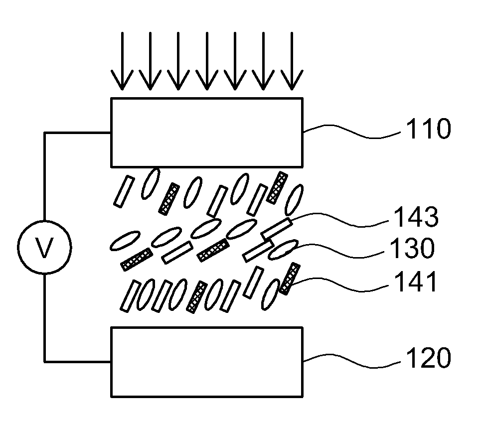
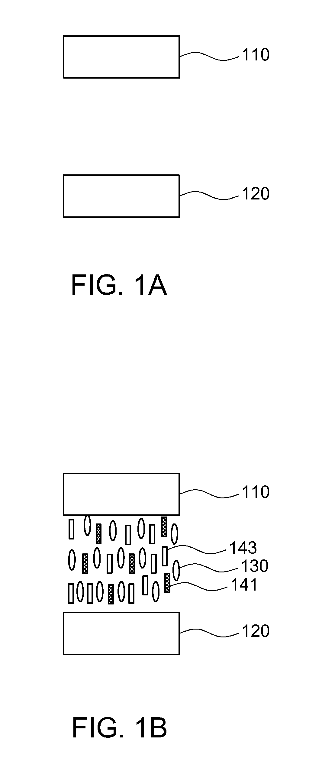
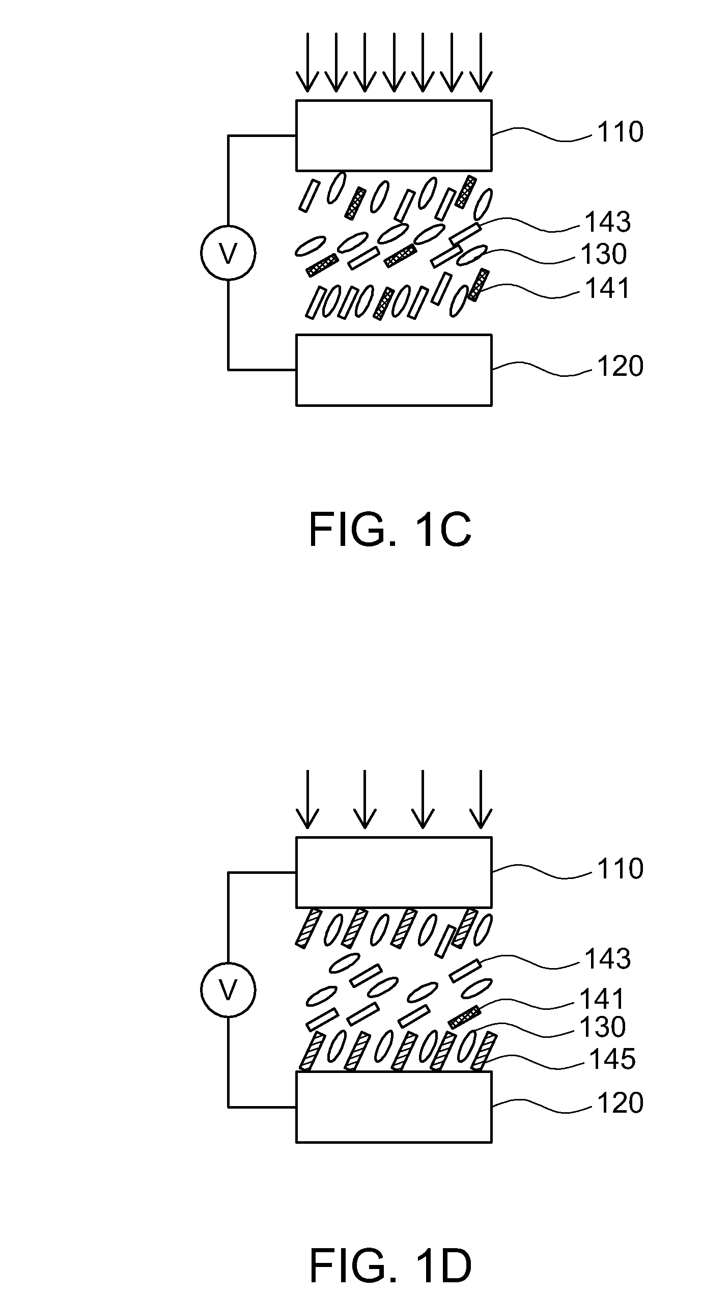
[0014]As indicated in the experimental results provided by the inventor, the more residual photosensitive monomers an LCD panel has, the worse the problems of luminance uniformity and image sticking will be. The inventor concludes that luminance non-uniformity and image sticking occur when the photosensitive monomers of an LCD panel are not completely polymerized as a polymer, and impurity substances such as photosensitive monomers are filled in the liquid crystal material and cause negative impact on the reaction of liquid crystal molecules. Thus, the invention provides a method of manufacturing an LCD panel. According to the manufacturing method of the invention, two processes of polymerization reaction are applied, such that the photosensitive monomers are completely polymerized as a polymer and will not be left in the liquid crystal material. Thus, luminance non-uniformity and image sticking can be improved. Particularly, in the second polymerization reaction the ultra-violet ha...


PUM

PropertyMeasurementUnit
wavelengthaaaaaaaaaa
second wavelengthaaaaaaaaaa
ultra-violet wavelengthaaaaaaaaaa

Abstract

A method for manufacturing a liquid crystal display (LCD) panel is provided. The method comprises the following steps. Firstly, an upper substrate and a lower substrate are provided. Next, a liquid crystal material is interposed between the upper and lower substrates. The liquid crystal material comprises at least one liquid crystal molecule and at least two photosensitive monomers, and the absorption peak of at least one photosensitive monomer is larger than 300 nm. Then, a voltage is applied between the upper substrate and the lower substrate, and a ultra-violet with a first wavelength is used for irradiation so as to allow most photosensitive monomers to be polymerized as polymer. Lastly, a ultra-violet with a second wavelength is used for irradiation, wherein the second wavelength is larger than the first wavelength so as to allow residual photosensitive monomers to be polymerized.

Description

[0001]This application claims the benefit of Taiwan application Serial No. 97133812, filed Sep. 3, 2008, the subject matter of which is incorporated herein by reference.BACKGROUND OF THE INVENTION[0002]1. Field of the Invention[0003]The invention relates in general to a liquid crystal display (LCD) panel and a method for manufacturing the same, and more particularly to an LCD panel using polymer-stabilizing alignment technology and a method for manufacturing the same.[0004]2. Description of the Related Art[0005]In recent years, alignment technology such as polymer-stabilizing alignment (PSA) technology is used in manufacturing LCD panel. According to the PSA technology, photosensitive monomers are mixed in a liquid crystal layer, and after the photosensitive monomers are arranged, an energy source such as ultra-violet or heat is applied to allow photosensitive monomers to be polymerized as a polymer to guide the arrangement of liquid crystal molecules.[0006]However, the LCD panel us...

Claims


Application Information

Patent Timeline
Patent Type & Authority Applications(United States)
IPC IPC(8): G02F1/1337
CPCC09K19/12C09K19/32C09K19/322C09K2019/0448C09K2019/122G02F2202/023G02F1/133788G02F2001/133397G02F2001/133715G02F2001/13775G02F2202/022G02F1/133711G02F1/133397G02F1/133715G02F1/13775
Inventor HSIEH, CHUNG-CHINGPAI, CHIA-HSUANHUANG, CHENG-WEICHEN, TE-SHENGSUGIURA, NORIO
Owner AU OPTRONICS CORP
Why Eureka
Try Eureka