Nanowire layer adhesion on a substrate

a technology of nanowires and substrates, applied in the field of nanotechnology, can solve the problems of increasing contact resistance, reducing the durability of electronic products, and difficult film use in electronic products requiring flexibility

Inactive Publication Date: 2010-03-04
SEOUL NAT UNIV R&DB FOUND
View PDF0 Cites 3 Cited by
  • Summary
  • Abstract
  • Description
  • Claims
  • Application Information

AI Technical Summary

Problems solved by technology

While crystalline thin films such as ITO, and the like, exhibit adhesive strength with the substrate, such films may be difficult to employ in electronic products requiring flexibility.
On the other hand, conventional flexible thin films formed, for example, from nano fibers, tend to exhibit weaker adhesive strength between the nano fiber and the substrate, thereby reducing the durability of the electronic products and increasing contact resistance, resulting in deterioration of the electrical characteristics of the products.

Method used


Image

  • Nanowire layer adhesion on a substrate
  • Nanowire layer adhesion on a substrate
  • Nanowire layer adhesion on a substrate

Examples


Embodiment Construction

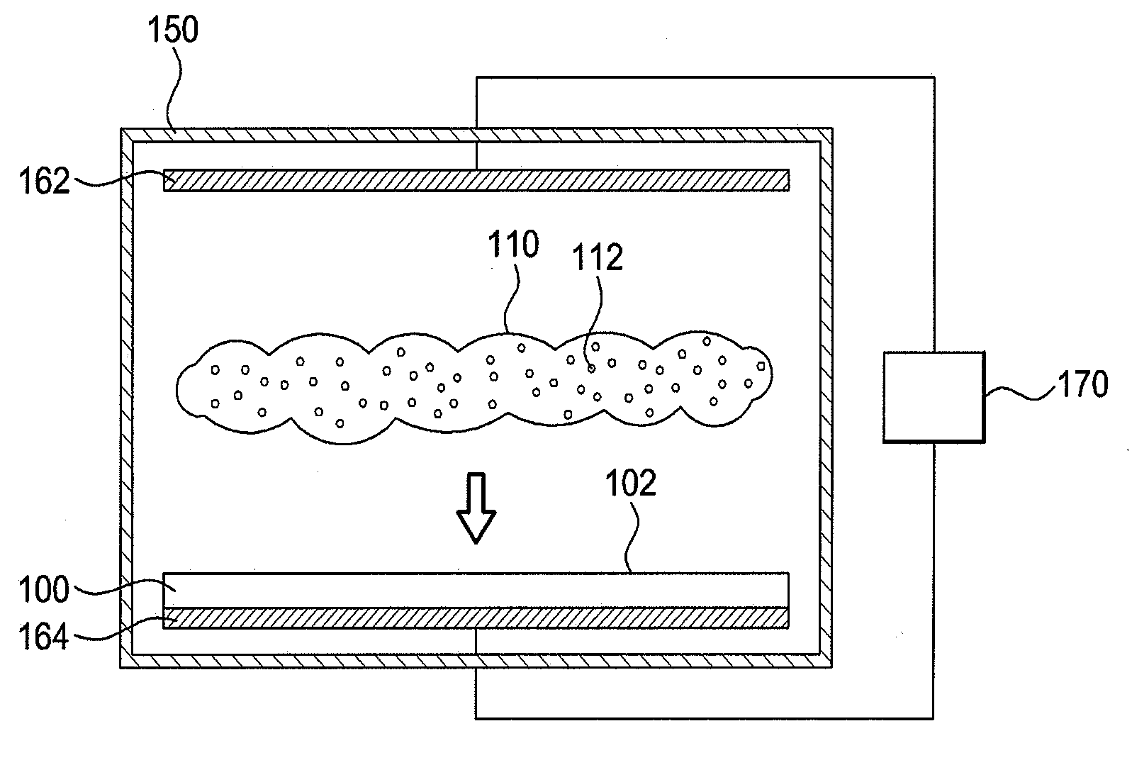
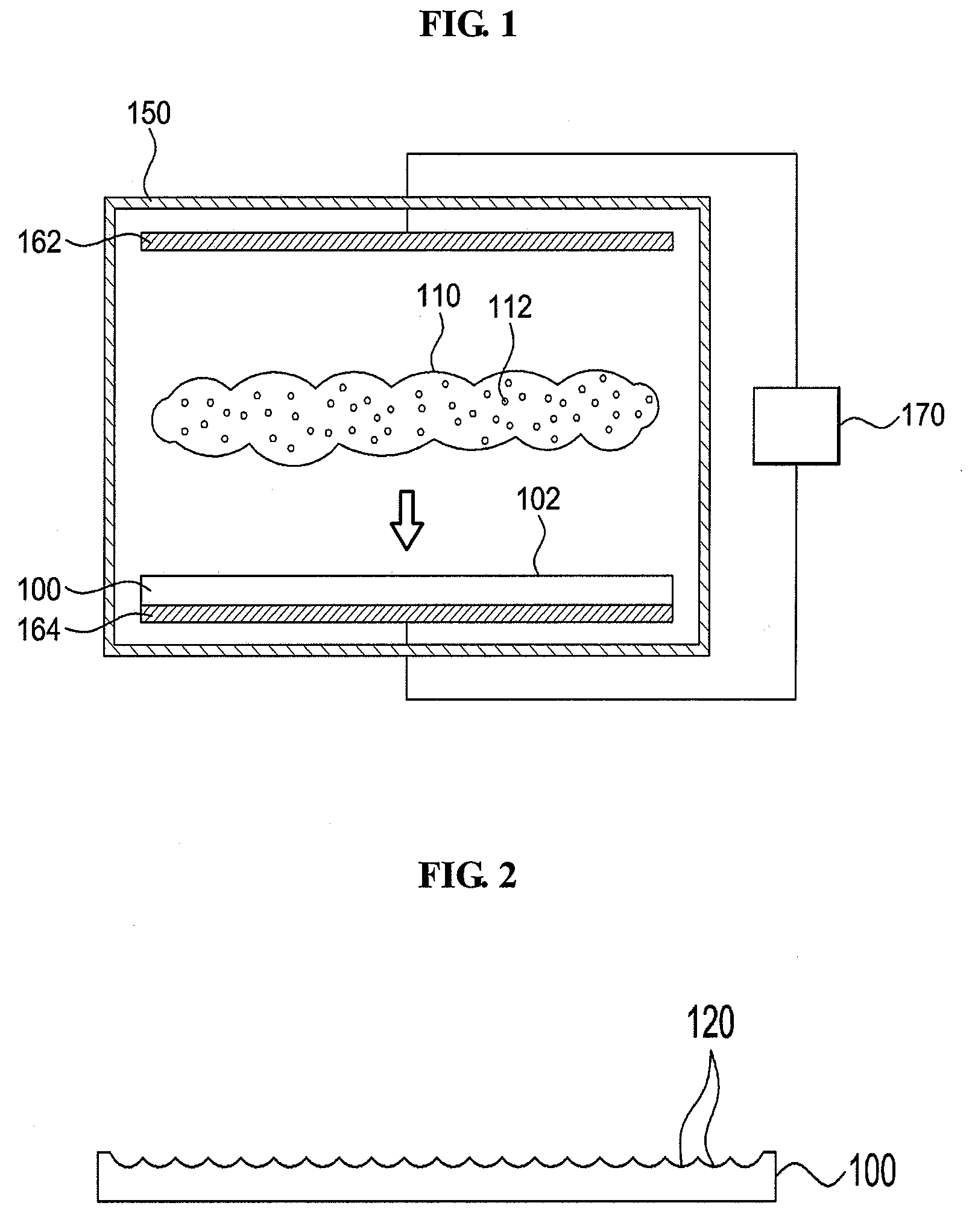
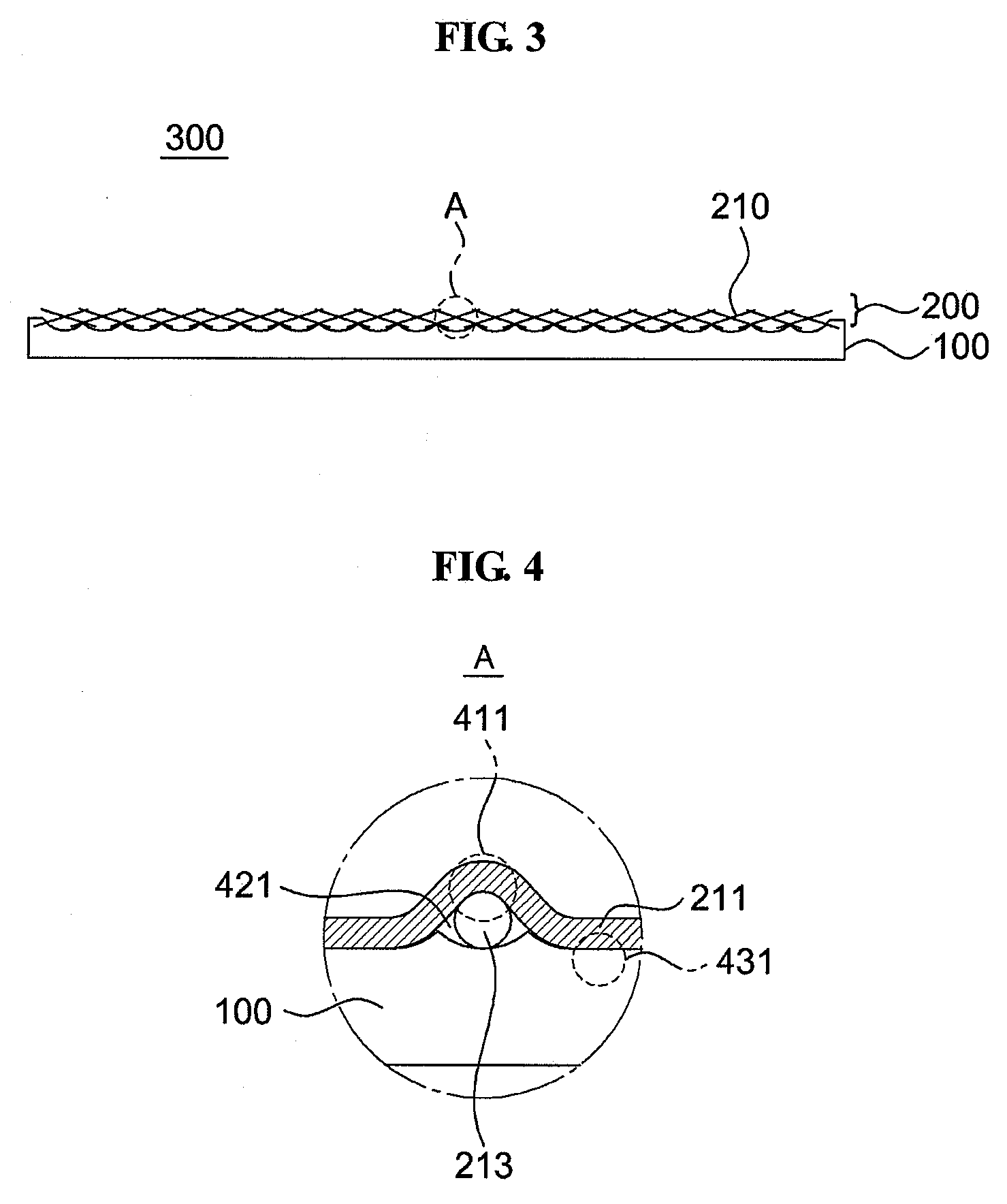
[0017]In the following detailed description, reference is made to the accompanying drawings, which form a part hereof. In the drawings, similar symbols typically identify similar components, unless context dictates otherwise. The illustrative embodiments described in the detailed description, drawings, and claims are not meant to be limiting. Other embodiments may be utilized, and other changes may be made, without departing from the spirit or scope of the subject matter presented here. It will be readily understood that the components of the present disclosure, as generally described herein, and illustrated in the Figures, may be arranged, substituted, combined, and designed in a wide variety of different configurations, all of which are explicitly contemplated and make part of this disclosure.

[0018]The embodiment(s) described, and references in the specification to “one embodiment”, “an embodiment”, “an example embodiment”, etc., indicate that the embodiment(s) described may inclu...


PUM

PropertyMeasurementUnit
electric poweraaaaaaaaaa
internal pressureaaaaaaaaaa

Abstract

Techniques for forming nanowire layers on a substrate are provided.

Description

BACKGROUND[0001]1. Technical Field[0002]The present disclosure relates generally to nanotechnology and, more particularly, to nanowire layer adhesion.[0003]2. Description of Related Art[0004]The current trend of electronic products becoming smaller and thinner has led to the use of various thin film members. In general, thin films may be formed using deposition methods such as sputtering, vapor deposition, and the like.[0005]As a representative thin film member, a transparent electrode may be manufactured by depositing transparent conductive materials such as Indium Tin Oxide (ITO) on a transparent substrate.[0006]While crystalline thin films such as ITO, and the like, exhibit adhesive strength with the substrate, such films may be difficult to employ in electronic products requiring flexibility.[0007]On the other hand, conventional flexible thin films formed, for example, from nano fibers, tend to exhibit weaker adhesive strength between the nano fiber and the substrate, thereby re...

Claims


Application Information

Patent Timeline
Patent Type & Authority Applications(United States)
IPC IPC(8): H01M4/02H01B13/004C23C14/02B32B5/16
CPCH01M4/02H01M4/0402H01M4/48Y10T428/25H01M4/96Y02E60/50H01M4/583Y02E60/10
Inventor KIM, YONG HYUPJANG, EUI YUN
Owner SEOUL NAT UNIV R&DB FOUND
Why Eureka
Try Eureka