Nitride-based semiconductor device and method of manufacturing the same

a technology of nitride-based semiconductors and manufacturing methods, which is applied in the direction of sustainable manufacturing/processing, semiconductor lasers, final product manufacturing, etc., can solve the problems of annealing of hf layer and al layer, and achieve the effect of suppressing the ohmic contact characteristics due to thermal treatment (thermal treatment temperature) for alloying

Inactive Publication Date: 2010-03-11
SANYO ELECTRIC CO LTD
View PDF4 Cites 33 Cited by
  • Summary
  • Abstract
  • Description
  • Claims
  • Application Information

AI Technical Summary

Benefits of technology

[0027]In the aforementioned method of manufacturing a nitride-based semiconductor device according to the second aspect, the step of forming the n-side electrode preferably includes a step of forming the n-side electrode without thermal treatment after stacking the first and second metal layers. According to this structure, the n-side electrode can be formed without thermal treatment for alloying the first and second metal layers at a constant ratio by controlling a prescribed temperature condition or time after stacking the first and second metal layers, and hence deterioration of the ohmic contact characteristics due to thermal treatment (thermal treatment temperature) for alloying can be suppressed.
[0028]The aforementioned method of manufacturing a nitride-based semiconductor device according to the second aspect preferably further comprises a step of thinning of said n-type semiconductor layer from a side of the surface of the n-type nitride-based semiconductor layer in advance of the step of forming the n-side electrode, and a step of removing a surface layer generated on the surface of the n-type nitride-based semiconductor layer by thinning. According to this structure, when forming the n-side electrode, the first metal layer can be formed on the surface of the n-type nitride-based semiconductor layer cleaned by removing the surface layer generated by thinning, and hence adhesiveness between the n-type nitride-based semiconductor layer and the n-side electrode (first metal layer) can be improved.

Problems solved by technology

In the nitride-based semiconductor device and the method of manufacturing the same disclosed in the aforementioned Japanese Patent Laying-Open No. 2003-142732, however, a step of alloying Hf and Al by stacking the Hf layer and the Al layer on the surface of the n-type nitride-based semiconductor layer in this order and thereafter annealing the Hf layer and the Al layer at the prescribed temperature is disadvantageously required in order to obtain the excellent ohmic contact.

Method used


Image

  • Nitride-based semiconductor device and method of manufacturing the same
  • Nitride-based semiconductor device and method of manufacturing the same
  • Nitride-based semiconductor device and method of manufacturing the same

Examples


embodiments

[0050]Embodiments of the present invention will be hereinafter described with reference to the drawings.

first embodiment

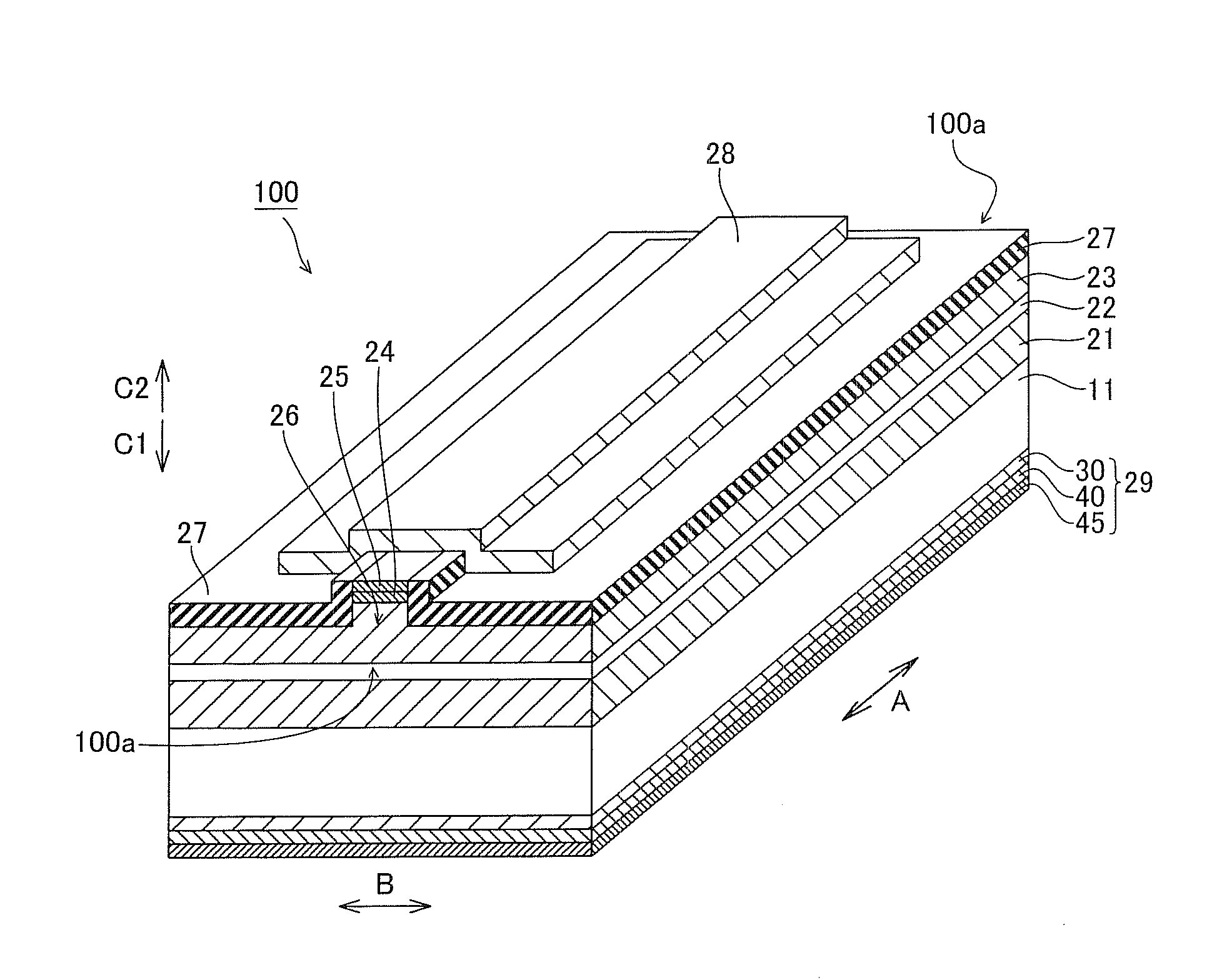
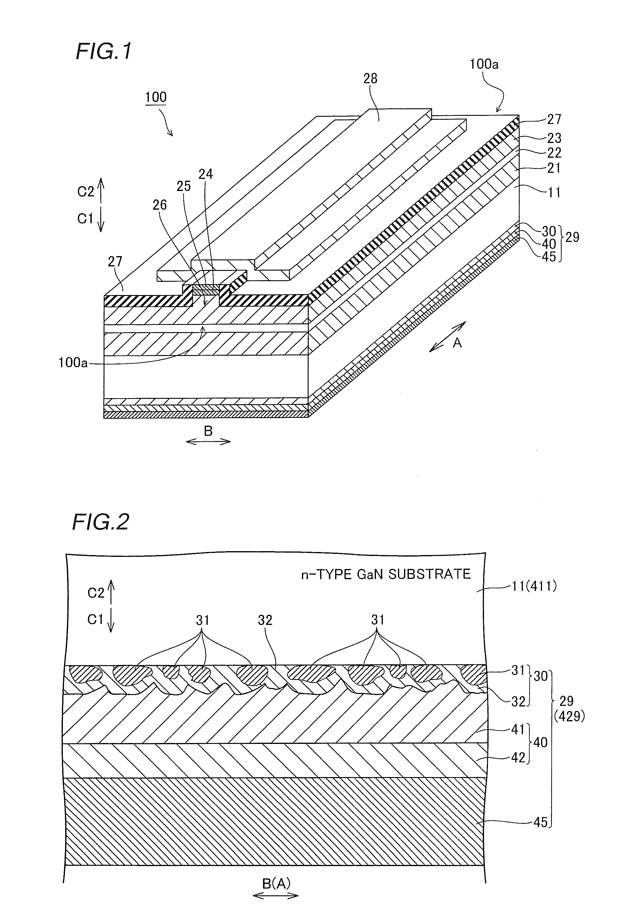
[0051]A structure of a blue-violet semiconductor laser device 100 according to a first embodiment of the present invention will be now described with reference to FIGS. 1 to 3. According to the first embodiment, the present invention is applied to the blue-violet semiconductor laser device 100 which is an exemplary nitride-based semiconductor laser device. The blue-violet semiconductor laser device 100 is an example of the “semiconductor light-emitting device” in the present invention.

[0052]In the blue-violet semiconductor laser device 100 according to the first embodiment of the present invention, an n-type cladding layer 21 made of n-type AlGaN is formed on an n-type GaN substrate 11 made of GaN as shown in FIG. 1. An active layer 22 having a multiple quantum well (MQW), obtained by alternately stacking four barrier layers (not shown) consisting of undoped GaInN and three well layers (not shown) consisting of undoped GaInN is formed on the n-type cladding layer 21. A p-type claddi...

second embodiment

[0078]Referring to FIGS. 5 and 6, according to a second embodiment, a blue-violet semiconductor laser device portion 110 is bonded to a surface of a p-type Ge substrate 50 through a conductive fusible layer 1, dissimilarly to the aforementioned first embodiment. The p-type Ge substrate 50 is an example of the “support substrate” in the present invention.

[0079]In a semiconductor laser device 200 according to the second embodiment of the present invention, a blue-violet semiconductor laser device portion 110 having a thickness of about 5 μm is bonded to an upper surface of the p-type Ge substrate 50 having a thickness of about 100 μm through a fusible layer 1, as shown in FIG. 5.

[0080]In the blue-violet semiconductor laser device portion 110, an active layer 22 obtained by alternately stacking four barrier layers (not shown) and three well layers (not shown), a p-type cladding layer 23 and a p-type contact layer 24 are formed in this order on a lower surface of an n-type cladding laye...


PUM

PropertyMeasurementUnit
thicknessaaaaaaaaaa
thicknessaaaaaaaaaa
thicknessaaaaaaaaaa

Abstract

A nitride-based semiconductor device includes an n-type nitride-based semiconductor layer, and an n-side electrode having a first metal layer made of Al, formed on a surface of the n-type nitride-based semiconductor layer and a second metal layer made of Hf formed so as to cover a surface of the first metal layer on a side opposite to the n-type nitride-based semiconductor layer.

Description

CROSS-REFERENCE TO RELATED APPLICATIONS[0001]The priority application number JP2008-233909, Nitride-Based Semiconductor Device and Method of Manufacturing the Same, Sep. 11, 2008, Kunio Takeuchi, upon which this patent application is based is hereby incorporated by reference.BACKGROUND OF THE INVENTION[0002]1. Field of the Invention[0003]The present invention relates to a nitride-based semiconductor device and a method of manufacturing the same, and more particularly, it relates to a nitride-based semiconductor device comprising an electrode formed on a surface of an n-type nitride-based semiconductor layer and a method of manufacturing the same.[0004]2. Description of the Background Art[0005]A nitride-based semiconductor device comprising an electrode formed on a surface of an n-type nitride-based semiconductor layer and a method of manufacturing the same is known in general, as disclosed in Japanese Patent Laying-Open No. 2003-142732, for example.[0006]The aforementioned Japanese ...

Claims


Application Information

Patent Timeline
Patent Type & Authority Applications(United States)
IPC IPC(8): H01L33/00H01L31/0224H01L31/0264H01L21/20
CPCB82Y20/00Y02E10/544H01L29/452H01L31/022425H01L31/022466H01L31/0304H01L31/184H01L33/32H01L33/40H01S5/0014H01S5/0202H01S5/0216H01S5/0217H01S5/028H01S5/0425H01S5/22H01S5/2214H01S5/34333H01L29/2003H01L31/022475H01S5/04252H01S5/04254Y02P70/50
Inventor TAKEUCHI, KUNIO
Owner SANYO ELECTRIC CO LTD
Why Eureka
Try Eureka