Electronic ballast having a partially self-oscillating inverter circuit

a technology of inverter circuit and electronic ballast, which is applied in the field of electronic ballasts, can solve the problems of not being suitable for residential installations, difficult to install and service, and expensive prior art ballasts

Active Publication Date: 2010-03-11
LUTRON TECH CO LLC
View PDF18 Cites 20 Cited by
  • Summary
  • Abstract
  • Description
  • Claims
  • Application Information

AI Technical Summary

Benefits of technology

[0007]According to an embodiment of the present invention, an electronic ballast for driving a gas discharge lamp comprises a bus capacitor for producing a substantially DC bus voltage, an inverter circuit for converting the DC bus voltage to a high-frequency AC voltage for driving the lamp, and a control circuit. The inverter circuit comprises a main transformer having a primary winding for producing the high-frequency AC voltage, first and second semiconductor switches electrically coupled to the primary winding of the main transformer for conducting current t...

Problems solved by technology

This has caused most prior art ballasts to be rather expensive and fairly dif...

Method used


Image

  • Electronic ballast having a partially self-oscillating inverter circuit
  • Electronic ballast having a partially self-oscillating inverter circuit
  • Electronic ballast having a partially self-oscillating inverter circuit

Examples


first embodiment

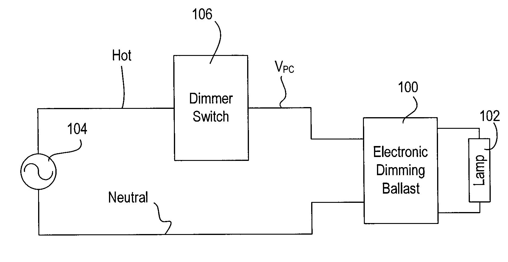
[0035]FIG. 1 is a simplified block diagram of a system including an electronic dimming ballast 100 for driving a fluorescent lamp 102 according to the present invention. The ballast 100 is coupled to the hot side of an alternating-current (AC) power source 104 (e.g., 120 VAC, 60 Hz) through a conventional two-wire dimmer switch 106. The dimmer switch 106 typically includes a bidirectional semiconductor switch (not shown), such as, for example, a triac or two field-effect transistors (FETs) coupled in anti-series connection, for providing a phase-controlled voltage VPC (i.e., a dimmed-hot voltage) to the ballast 100. Using a standard forward phase-control dimming technique, the bidirectional semiconductor switch is rendered conductive at a specific time each half-cycle of the AC power source and remains conductive for a conduction period TCON during each half-cycle. The dimmer switch 106 is operable to control the amount of power delivered to the ballast 100 by controlling the length...

second embodiment

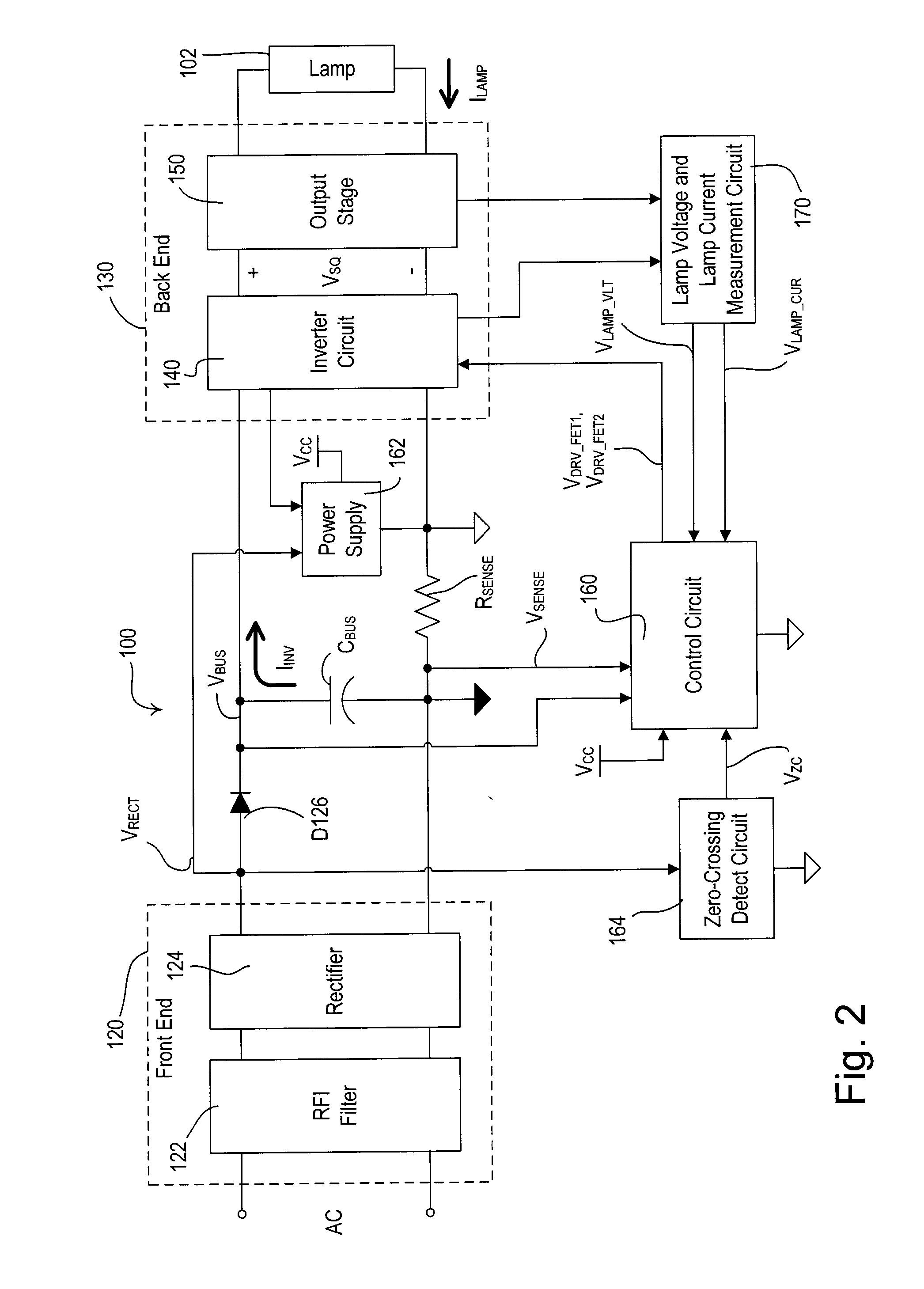
[0108]FIG. 13 is a simplified block diagram of an electronic dimming ballast 1000 according to the present invention. The electronic dimming ballast 1000 comprises a charge pump circuit 1010, which is coupled in parallel electrical connection the diode D126 between the rectifier 124 and the inverter circuit 140. When the magnitude of the rectified voltage VRECT is less than the magnitude of the bus voltage VBUS, the charge pump circuit 1010 operates to draw a charge current ICP from the AC power source 104. Specifically, the charge pump circuit 1010 is coupled to the output of the inverter circuit 140, such that the charge pump circuit 1010 is operable to draw the charge current ICP every other half-cycle of the square-wave voltage VSQ. The charge current ICP drawn during the times that the magnitude of the rectified voltage VRECT is less than the magnitude of the bus voltage VBUS helps to prevent the current through the triac of the dimmer switch 106 from dropping below the holding...

third embodiment

[0112]FIG. 15 is a simplified schematic diagram of a lamp current measurement circuit 420′ of the measurement circuit 170 according to the present invention. A current transformer 270′ has two primary winding coupled between the resonant tank circuit 150 and to the lamp 102 as shown in FIG. 4. However, the current transformer 270′ only has a single secondary winding coupled to the lamp current measurement circuit 420′. Specifically, the secondary winding of the current transformer 270′ is coupled across the base-emitter junction of a PNP bipolar junction transistor Q1510. The junction of the base of the transistor Q1510 and the secondary winding of the current transformer 270′ is coupled to the DC supply voltage VCC. When the lamp current ILAMP (and thus the current through the secondary winding of the current transformer 270′) has a positive magnitude, the transistor Q1110 is rendered conductive, thus conducting current through a capacitor C1512 and a resistor R1514. The lamp curre...


PUM


Abstract

An electronic ballast for driving a gas discharge lamp comprises an inverter circuit that operates in a partially self-oscillating manner. The inverter circuit comprises a push-pull converter having a main transformer having a primary winding for producing a high-frequency AC voltage, semiconductor switches electrically coupled to the primary winding of the main transformer for conducting current through the primary winding on an alternate basis, and gate drive circuits for controlling the semiconductor switches on a cycle-by-cycle basis. The drive circuits control (e.g., turn on) the semiconductor switches in response to first control signals derived from the main transformer, and control (e.g., turn off) the semiconductor switches in response to second control signals received from a control circuit. The control circuit controls the semiconductor switches in response to a peak value of an integral of an inverter current flowing through the inverter circuit.

Description

BACKGROUND OF THE INVENTION[0001]1. Field of the Invention[0002]The present invention relates to electronic ballasts for gas discharge lamps, such as fluorescent lamps. More specifically, the present invention relates to a two-wire electronic dimming ballast for powering and controlling the intensity of a fluorescent lamp in response to a phase-controlled voltage.[0003]2. Description of the Related Art[0004]The use of gas discharge lamps, such as fluorescent lamps, as replacements for conventional incandescent lamps, has increased greatly over the last several years. Fluorescent lamps typically are more efficient and provide a longer operational life when compared to incandescent lamps. In certain areas, such as California, for example, state law requires certain areas of new construction to be outfitted for the use of fluorescent lamps exclusively.[0005]A gas discharge lamp must be driven by a ballast in order to illuminate properly. The ballast receives an alternating-current (AC)...

Claims


Application Information

Patent Timeline
IPC IPC(8): H05B41/36
CPCH05B41/295
Inventor NEWMAN, JR., ROBERT C.TAIPALE, MARK S.
Owner LUTRON TECH CO LLC
Why Eureka
Try Eureka