Method of Separating Light-Emitting Diode from a Growth Substrate

a technology of light-emitting diodes and growth substrates, which is applied in the direction of vacuum evaporation coatings, solid-state devices, coatings, etc., can solve the problems of high cost, high cost, and high cost of separation process, and achieve the effect of reducing the cost of separation

Active Publication Date: 2010-03-11
EPISTAR CORP
View PDF5 Cites 20 Cited by
  • Summary
  • Abstract
  • Description
  • Claims
  • Application Information

AI Technical Summary

Problems solved by technology

The separating process can be very time-consuming, especially for separating large area films, and are economically unfavorable for manufacturing processes of large scale.
The process, however, suffers various difficulties.
As an example, the high energy laser radiation may blow away the overlying GaN film, and fracturing of the GaN film often occurs.
Moreover, the area of the high-energy laser beams is limited, which makes separating large area films difficult.

Method used


Image

  • Method of Separating Light-Emitting Diode from a Growth Substrate
  • Method of Separating Light-Emitting Diode from a Growth Substrate
  • Method of Separating Light-Emitting Diode from a Growth Substrate

Examples


Embodiment Construction

[0015]The making and using of the presently preferred embodiments are discussed in detail below. It should be appreciated, however, that the present invention provides many applicable inventive concepts that can be embodied in a wide variety of specific contexts. The specific embodiments discussed are merely illustrative of specific ways to make and use the invention, and do not limit the scope of the invention.

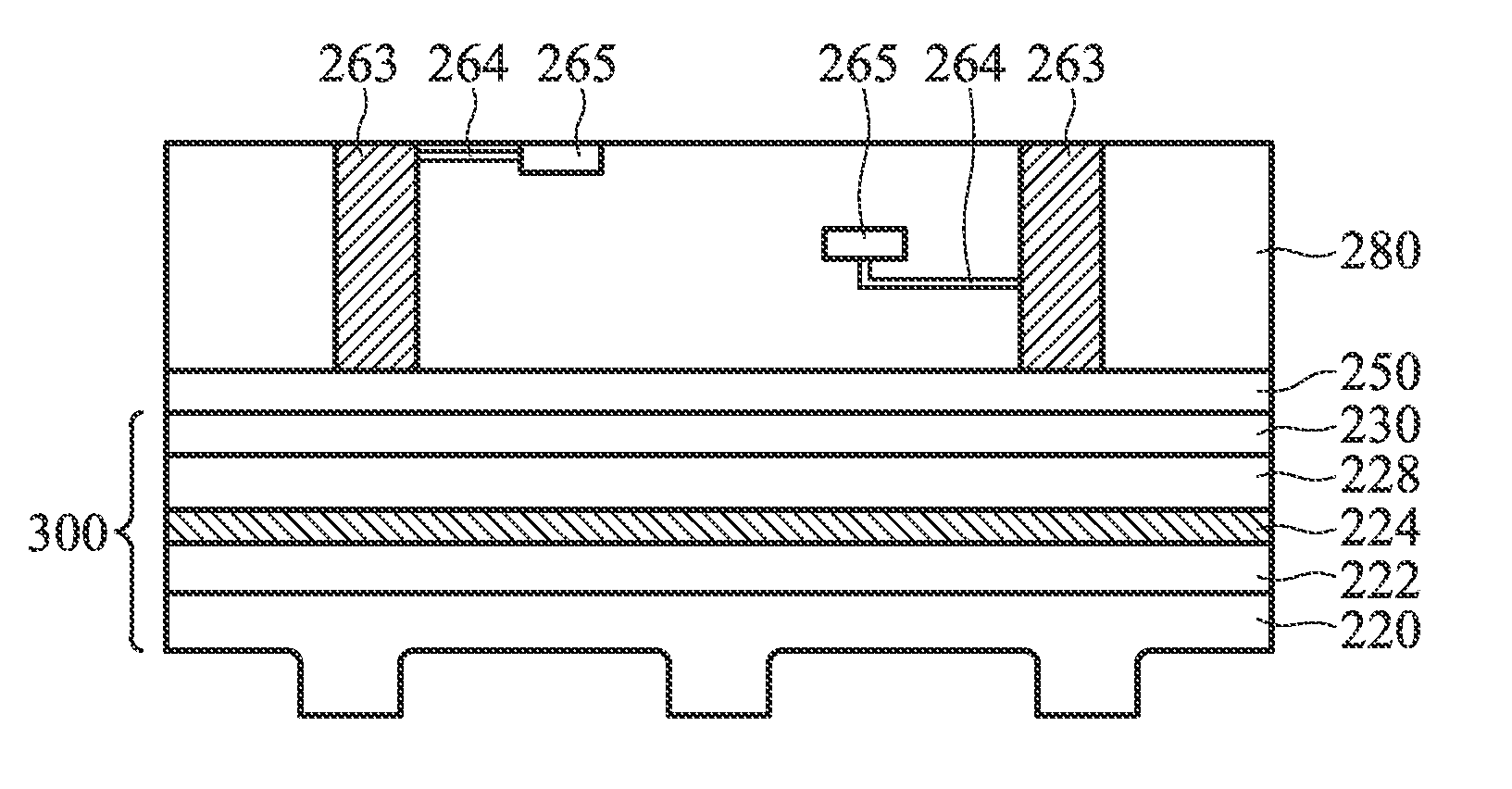
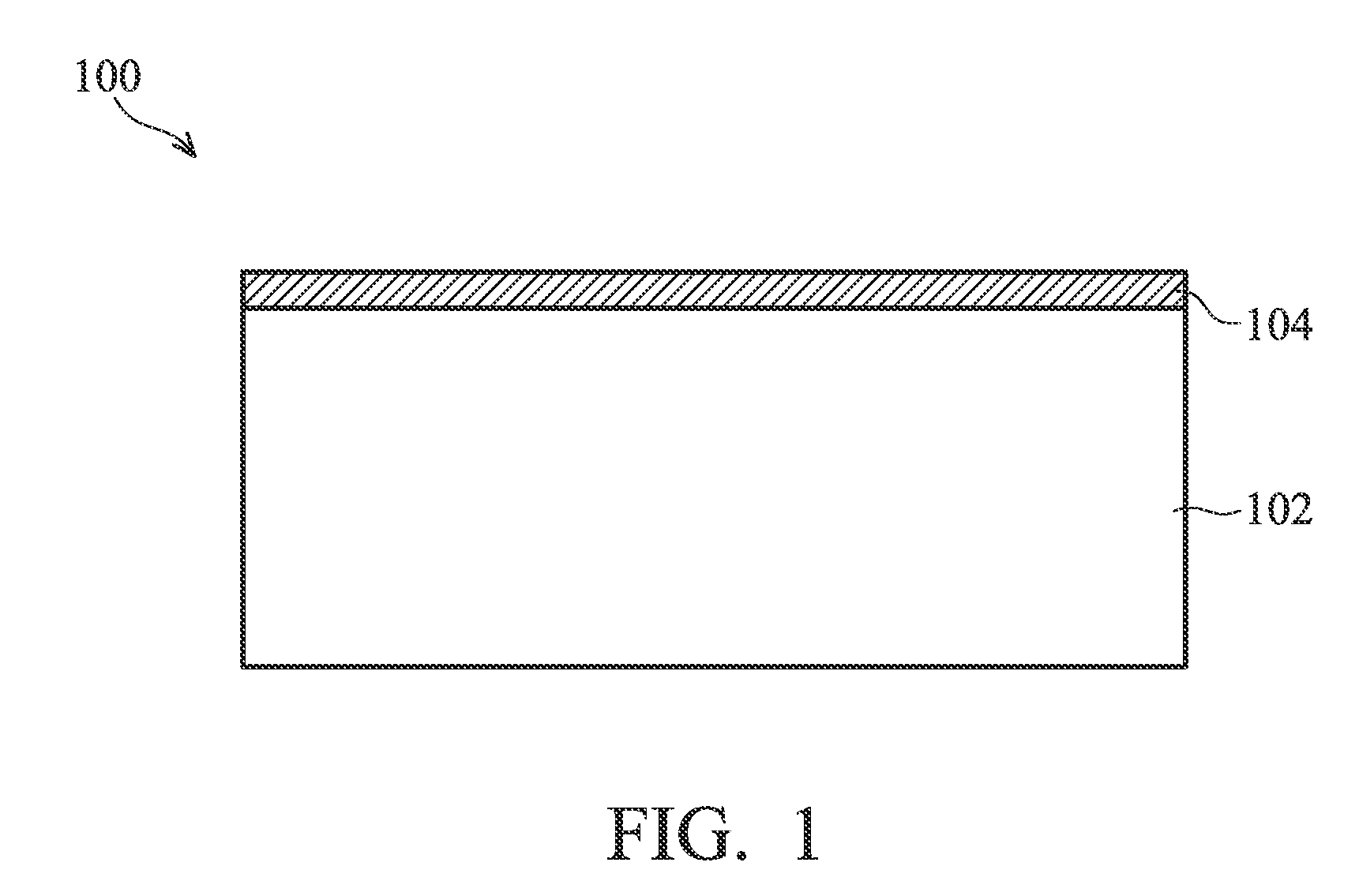
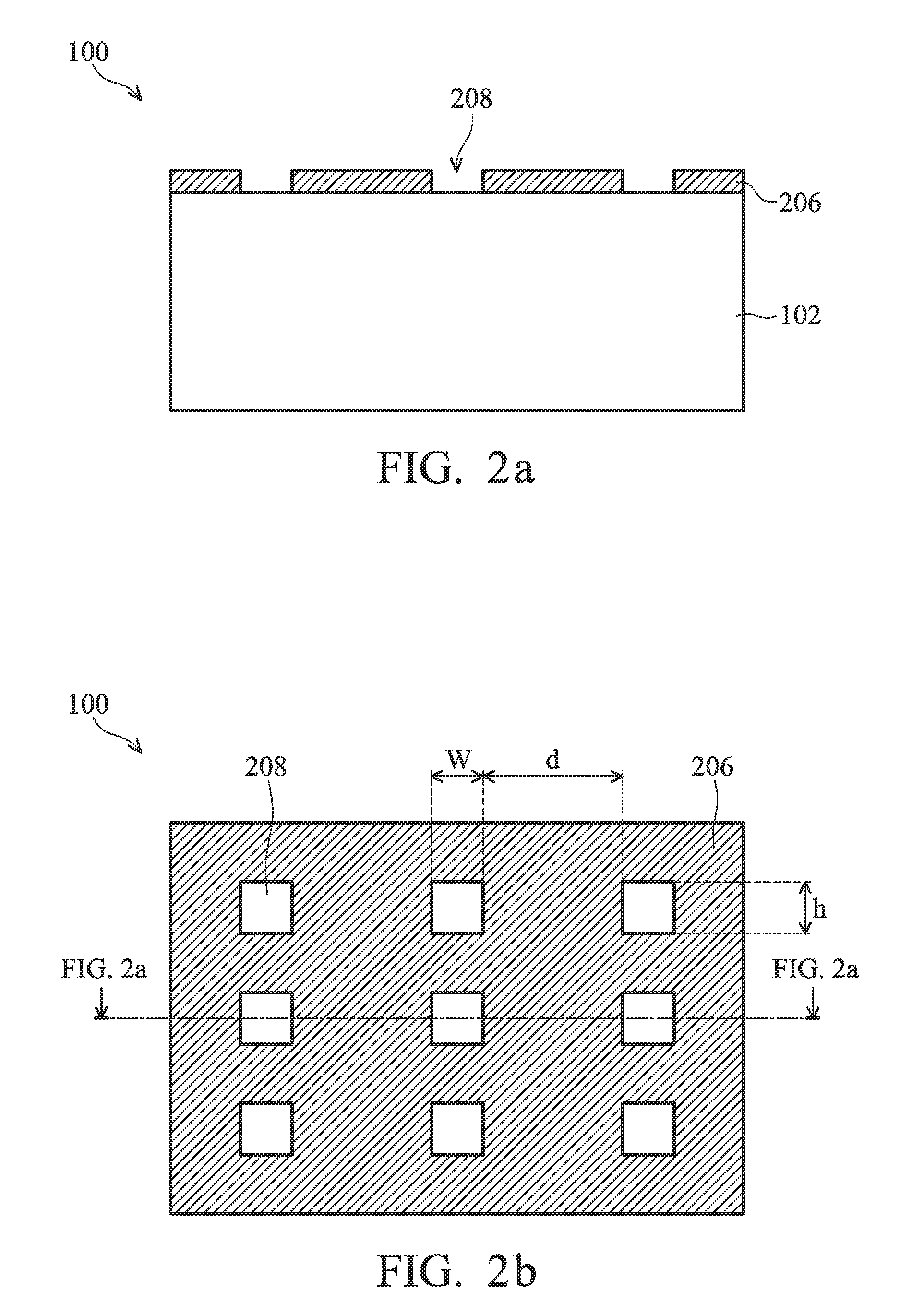
[0016]A novel method for forming GaN layers for light-emitting diodes (LEDs) and separating the LEDs from a growth substrate is provided. The intermediate stages of manufacturing preferred embodiments of the present invention are illustrated. It should be understood that the shown steps illustrate the inventive aspects of the invention, but other processes may be performed. Throughout the various views and illustrative embodiments of the present invention, like reference numbers are used to designate like elements.

[0017]FIGS. 1-6 illustrate various intermediate process steps ...


PUM

PropertyMeasurementUnit
height widthaaaaaaaaaa
distanceaaaaaaaaaa
depthaaaaaaaaaa

Abstract

A method of forming a light-emitting diode (LED) device and separating the LED device from a growth substrate is provided. The LED device is formed by forming an LED structure over a growth substrate. The method includes forming and patterning a mask layer on the growth substrate. A first contact layer is formed over the patterned mask layer with an air bridge between the first contact layer and the patterned mask layer. The first contact layer may be a contact layer of the LED structure. After the formation of the LED structure, the growth substrate is detached from the LED structure along the air bridge.

Description

[0001]This application claims the benefit of U.S. Provisional Application No. 61 / 095,773, filed on Sep. 10, 2008, entitled Method of Separating Light-Emitting Diode from a Growth Substrate, and U.S. Provisional Application No. 61 / 147,677, filed on Jan. 27, 2009, entitled Method of Separating Light-Emitting Diode from a Growth Substrate which applications are hereby incorporated herein by reference.TECHNICAL FIELD[0002]This invention relates generally to semiconductor device manufacturing processes and, more particularly, to forming a light-emitting diode and separating a light-emitting diode structure from a growth substrate.BACKGROUND[0003]Compound semiconductor devices are widely used for optoelectronic applications. For example, compound semiconductors composed of materials from group III-V are best suitable for light-emitting diodes (LEDs). LEDs are manufactured by forming active regions on a substrate and by depositing various conductive and semiconductive layers on the substra...

Claims


Application Information

Patent Timeline
Patent Type & Authority Applications(United States)
IPC IPC(8): H01L27/15
CPCH01L21/0254H01L21/0262H01L21/02639H01L33/0079H01L25/167H01L33/007H01L21/0265C23C14/048H01L2924/0002H01L33/0093H01L2924/00
Inventor CHEN, DING-YUANLIN, HUNG-TAYU, CHEN-HUACHIOU, WEN-CHIH
Owner EPISTAR CORP
Why Eureka
Try Eureka