Heterojunction bipolar transistor and its fabrication method

a bipolar transistor and heterojunction technology, applied in the field of bipolar transistors, can solve the problems of difficult control of the fabrication process of this structure, difficulty in raising the maximum usable oscillation frequency, and difficulty in achieving the effect of hbts in the related ar

Inactive Publication Date: 2002-05-28
LG ELECTRONICS INC
View PDF3 Cites 15 Cited by
  • Summary
  • Abstract
  • Description
  • Claims
  • Application Information

AI Technical Summary

Problems solved by technology

Thus, the HBT structure shown in FIGS. 1a and 1b limits the reduction of the widths W.sub.E and W, and the maximum usable oscillation frequency is difficult to raise.
However, controlling the fabrication process for this structure is difficult.
The HBTs in the related art have several problems.
First, it is difficult to control the exact point in time to stop etching the polyimide.
An excessive etching causes an electrical short at the emitter-base junction during the later metal wiring step.
Second, the etching has to be stopped at a moment the emitter electrode is exposed in the HBT fabrication process of in the related art.
However, it is difficult to automatically stop the etching utilizing an end point detector in the RIE equipment or to observe the end point with a microscope, because the emitter electrode is one of the smallest portion of the substrate.
Third, a separate mask is required to define the base-collector PN junction, which makes it difficult to minimize the width of the base-collector PN junction in the manner of self-alignment.

Method used


Image

  • Heterojunction bipolar transistor and its fabrication method
  • Heterojunction bipolar transistor and its fabrication method
  • Heterojunction bipolar transistor and its fabrication method

Examples


first embodiment

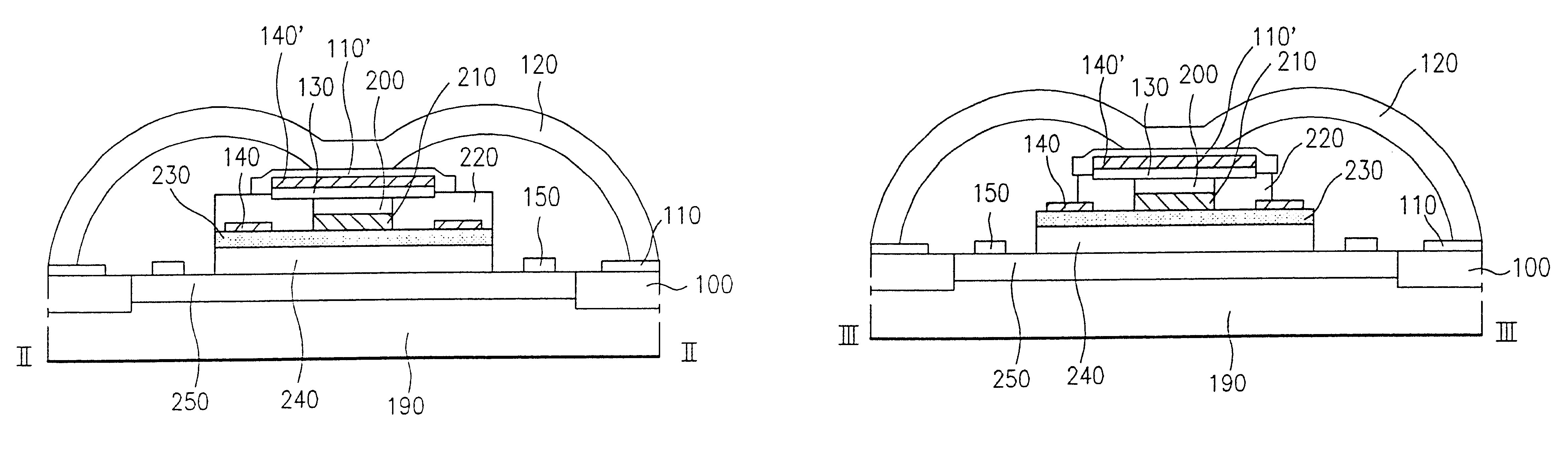
FIG. 5a is a plane view of an HBT according to the present invention, and FIG. 5b is a cross-sectional view of the HBT taken along the line II--II. A substrate 190 is composed of a normal semi-insulating semiconductor substrate and a sub-collector layer 250 is formed on the substrate 190. An insulating layer 100 is formed by implanting ions into the substrate as deep as a predetermined depth with respect to the sub-collector layer. A collector electrode 150 is formed in a defined profile on a portion of the sub-collector layer 250. A base layer 230 is deposited on a collector layer 240. An emitter layer 210 is formed in a defined profile on a part of the base layer 230, while an ohmic cap layer 200 is formed in the same profile as the emitter layer 210 on the emitter layer.

In the present invention, a base electrode 140 is formed in a defined profile at a position separated by a predetermined distance from the edge of the emitter layer on the base layer. An emitter electrode 130 cove...

second embodiment

FIGS. 8a-8e are cross-sectional views illustrating a fabrication process for the HBT according to the present invention. Referring to FIG. 8a, the procedures as described above in reference to FIGS. 6a-6h are repeated in the fabrication of the HBT shown in FIGS. 7a and 7b. The second insulating layer 220 and the emitter electrode 130 are used as a mask in etching the base layer 230 and the collector layer 240 to expose the sub-collector layer 250, as shown in FIG. 8b.

As shown in FIG. 8b, the electrode metal 110' is formed on the second insulating layer 220 to surround the base metal layer 140' on the emitter electrode 130. The second insulating layer 220 and the electrode metal 110' are used as an etching mask to define a base-collector PN junction. As shown in FIG. 8c, the electrode metal 110' is used as a mask in a second etching step for etching the second insulating layer 220. The etching technique utilized is a reactive ion etching using an oxygen plasma.

Subsequently, the colle...

third embodiment

the HBT has the a same structure as the first embodiment of the HBT with the exception of a first insulating layer sidewall 300' surrounding the ohmic cap layer and the emitter layer, and a depleted emitter layer 210' located under the first insulating layer. The fabrication procedures of FIG. 11i-11l are also analogous to those of FIGS. 6f-6j of the first embodiment.

Particularly, the depleted emitter layer 210' is formed in a defined profile on a portion of the base layer 230. The first insulating layer 300' surrounds the emitter layer 210 and the ohmic cap layer 200 with a height as high as the emitter layer 210 on the depleted emitter layer 210', while the second insulating layer is formed higher than the top surface of the ohmic cap layer 200 on the base layer 230 and the base electrode 140. "L" shown in FIG. 11f indicates the width of the depleted emitter layer 210' extending outside the boundary of emitter layer 210. The ledge (emitter surrounding band structure) protects the ...


PUM


Abstract

A heterojunction bipolar transistor and its fabrication method is disclosed. The heterojunction bipolar transistor includes a substrate; a collector layer formed to have a ledge or MESA on the substrate; a collector electrode formed on the collector layer surrounding the ledge; a base layer formed on the ledge of the collector layer; an ohmic cap layer on the emitter layer; an emitter layer formed in the center of the base layer; an emitter electrode formed on the ohmic cap layer; a base electrode formed on the base layer surrounding the emitter electrode; an insulating layer formed to cover the base electrode and to overlay on the insulating layer; a metal wire formed to cover the emitter electrode; and an air bridge brought in contact with the metal wire and electrically connected to an external pad lying on an ion-implanted isolation region.

Description

1. Field of the InventionThe present invention relates to a bipolar transistor and more particularly to a fully self-aligned heterojunction bipolar transistor (hereinafter, referred to as "HBT") with an overlay on the mask layout between the emitter and base electrodes.2. Discussion of Related ArtGenerally, HBTs are one of the most important transistors for the microwave frequency band which requires high speed characteristics. Both the emitter and the base of the HBTs are semiconductors, the emitter having a large energy band gap and the base having a small energy band gap. The difference in the energy band gap enables the HBTs to maintain a high current gain and to reduce the base series resistances by heavily doping the base with impurities. As a result, the HBTs have high speed characteristics.The HBTs are especially used in the field of power amplifiers over 1 GHz because HBTs have a high current density and a good linear property. The HBTs are also being used as a power amplif...

Claims


Application Information

Patent Timeline
Patent Type & Authority Patents(United States)
IPC IPC(8): H01L21/02H01L23/48H01L29/40H01L29/66H01L23/482H01L21/331H01L29/737H01L29/417H01L21/328
CPCH01L23/4821H01L29/41708H01L29/66242H01L29/7371H01L2924/0002H01L2924/00H01L21/18
Inventor SHIN, JIN HOLIM, TAE YUNKIM, HYUNG WOOK
Owner LG ELECTRONICS INC
Why Eureka
Try Eureka