Method for preparing air bridge using photosensitive subbing

A technology of air bridge and photosensitive adhesive, which is applied in the manufacture of electrical components, semiconductor/solid-state devices, circuits, etc., can solve the problems of poor controllability of chlorobenzene soaking process, low precision of air bridge, complicated process, etc., to avoid Ultrasonic or chemical corrosion process, protect the body health, reduce the effect of damage

Inactive Publication Date: 2008-10-01
INST OF MICROELECTRONICS CHINESE ACAD OF SCI
View PDF0 Cites 14 Cited by
  • Summary
  • Abstract
  • Description
  • Claims
  • Application Information

AI Technical Summary

Problems solved by technology

[0007] The quality of the air bridge made by this method is better, but the process of making the sacrificial rubber blocks supporting the air is complicate...

Method used


Image

  • Method for preparing air bridge using photosensitive subbing
  • Method for preparing air bridge using photosensitive subbing
  • Method for preparing air bridge using photosensitive subbing

Examples


Embodiment

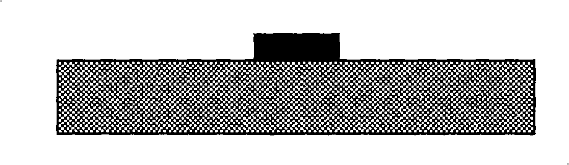
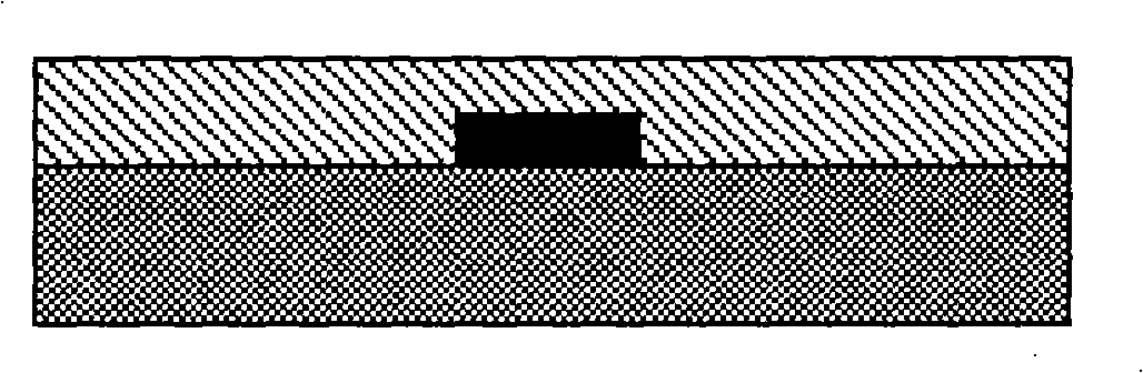
[0052] In this embodiment, 9918 is used as the sacrificial adhesive layer, AZ5214 photoresist is used as the secondary photoresist, and O2 plasma etching is used to remove the residual adhesive. The detailed process method and steps of the present invention will be further described below in conjunction with the specific process schematic diagram 2, and FIG. 7 is a schematic diagram of the process of making an air bridge in the present invention.

[0053] As shown in schematic diagram a in Figure 2, schematic diagram a is to apply a certain thickness of photoresist 9918 on the substrate to cover the underlying metal, with a thickness of 2.0 μm, and then bake at a temperature of 80 to 100 ° C for 70 to 110 seconds. For example, bake at 90°C for 90 seconds.

[0054] As shown in schematic diagram b in FIG. 2 , the substrate coated with photoresist 9918 is exposed under an exposure machine; for example, a contact exposure machine or a projection photolithography machine with G, H,...


PUM

PropertyMeasurementUnit
Thicknessaaaaaaaaaa

Abstract

The invention is related to a semiconductor device and the technical field of integrated circuit manufacturing process, and discloses a method for utilizing a photosensitive glue layer to manufacture air bridge, comprising the steps of: A, coating a sacrificed glue layer on a substrate to cover metal on the substrate, photo-etching, exposing and developing the coated sacrificed glue layer to form the air bridge support; B, baking the substrate which forms the air bridge support in order to smooth and solidify the edge corners f the sacrificed glue layer; C, coating secondary photo-etching glue on the substrate, photo-etching, exposing and developing the coated secondary photo-etching glue to form bridge surface; D, evaporating, sputtering and plating a layer of metal material on the substrate; E, peeling off the photo-etching glue on the substrate to form the air bridge. Usage of the invention can simplify the manufacturing process, improve controllability and precision of manufacturing, avoid the using of virulent reagent, and lessen damages of the device in the manufacturing process.

Description

technical field [0001] The invention relates to the technical field of manufacturing technology of semiconductor devices and integrated circuits, in particular to a method for making an air bridge by using a photosensitive adhesive layer. Background technique [0002] In the manufacturing process of modern semiconductor devices, as the circuit structure becomes more and more complex, one-time metal connection cannot meet the requirements, so multiple metal connections are often used for interconnection. But parasitics exist when metal lines cross or overlap each other. Since the dielectric constant of air is the smallest, the parasitic of intersecting or overlapping metal lines with air as the medium is the smallest. Therefore, in the manufacturing process of microelectronic devices and circuits, air is often used as the medium at the crossing or overlapping of some key metal lines. One metal wire straddles the air above another, so the structure is often called an air brid...

Claims


Application Information

Patent Timeline
IPC IPC(8): H01L21/768
Inventor 于进勇金智程伟刘新宇夏洋
Owner INST OF MICROELECTRONICS CHINESE ACAD OF SCI
Why Eureka
Try Eureka