AlGaN/GaN heterojunction multi-channel structure based terahertz schottky diode and manufacturing method therefor

A Schottky diode, terahertz Schottky technology, applied in diodes, semiconductor/solid-state device manufacturing, semiconductor devices, etc., can solve the problems of difficult SBD total series resistance Rs, low electron mobility, etc., to improve the cut-off frequency, the effect of reducing series resistance

Active Publication Date: 2016-06-15
XIDIAN UNIV
View PDF3 Cites 17 Cited by
  • Summary
  • Abstract
  • Description
  • Claims
  • Application Information

AI Technical Summary

Problems solved by technology

The current technical bottleneck lies in: In the traditional SBD structure, since the electron mobility of GaN material is significantly lower than that of GaAs, intentional doping makes the electron mobility lower, so it is extremely difficult to reduce the total series resistance Rs of SBD through the process, resulting in GaN The highest cut-off frequency of base SBD is obviously lower than that of GaAs base SBD

Method used


Image

  • AlGaN/GaN heterojunction multi-channel structure based terahertz schottky diode and manufacturing method therefor
  • AlGaN/GaN heterojunction multi-channel structure based terahertz schottky diode and manufacturing method therefor
  • AlGaN/GaN heterojunction multi-channel structure based terahertz schottky diode and manufacturing method therefor

Examples


Embodiment 1

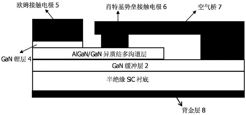
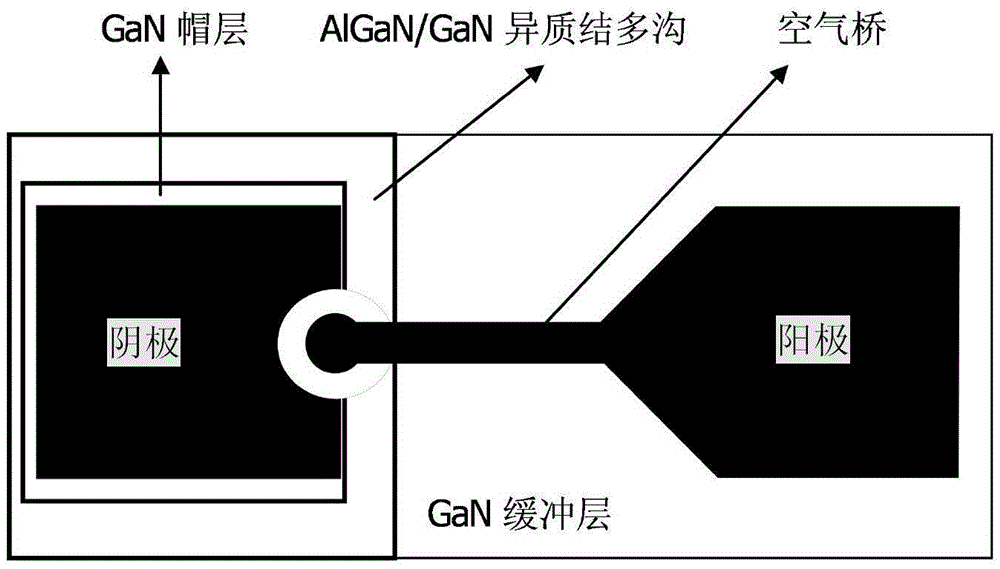
[0040] Fabrication of heterojunction dual-channel terahertz Schottky diodes on 4H-SiC semi-insulating substrate.

[0041] Step 1, put a 4H-SiC semi-insulating substrate with a diameter of 2 inches into the MOCVD reaction chamber, set the growth temperature at 930°C, and simultaneously feed trimethylgallium and nitrogen into the reaction chamber, and keep the pressure at 40Torr Under the condition of , a GaN buffer layer with a thickness of 2 μm was grown.

[0042] Step 2, injecting trimethylgallium and nitrogen gas into the reaction chamber at the same time, under the conditions of a pressure of 400 Torr and a temperature of 1000° C., a GaN channel layer with a thickness of 20 nm is epitaxially grown.

[0043] Step 3, feed trimethylgallium, nitrogen and trimethylaluminum into the reaction chamber at the same time, under the conditions of pressure of 400 Torr and temperature of 1060°C, epitaxial growth of AlGaN with a thickness of 10nm and an Al composition of 30% Layers.

[...

Embodiment 2

[0057] Example 2: Fabrication of a heterojunction dual-channel terahertz Schottky diode on a 6H-SiC semi-insulating substrate.

[0058] Step 1, epitaxial growth of GaN buffer layer:

[0059] Using MOCVD, under the conditions of maintaining a pressure of 40Torr and a temperature of 930°C, trimethylaluminum and nitrogen are introduced into the reaction chamber at the same time, and the thickness is grown on a 6H-SiC semi-insulating substrate with a diameter of 2 inches. 3μm GaN buffer layer.

[0060] Step 2, epitaxial growth of heterojunction double channel layer:

[0061] 3.1) Feed trimethylgallium and nitrogen into the reaction chamber at the same time, and epitaxially grow a GaN channel layer with a thickness of 10 nm under the conditions of a pressure of 400 Torr and a temperature of 1050 ° C;

[0062] 3.2) Feed trimethylgallium, nitrogen and trimethylaluminum into the reaction chamber at the same time, under the conditions of pressure 400Torr and temperature 1110°C, the c...

Embodiment 3

[0083] Embodiment 3: Fabricate a heterojunction four-channel Schottky diode on a 6H-SiC semi-insulating substrate.

[0084] Step A, making a GaN buffer layer:

[0085] Using MOCVD, under the conditions of maintaining a pressure of 40 Torr and a temperature of 930 °C, trimethylaluminum and nitrogen are simultaneously introduced into the reaction chamber, and a GaN buffer with a thickness of 2 μm is grown on a 6H-SiC semi-insulating substrate. layer.

[0086] Step B, epitaxial heterojunction four-channel layer:

[0087] Feed trimethylgallium, nitrogen and trimethylaluminum into the reaction chamber at the same time, and the feeding amount of trimethylaluminum first increases linearly and then stops feeding. Under the conditions of maintaining the pressure at 600 Torr and the temperature at 1100°C, The AlGaN / GaN-like superlattice is epitaxially grown for 4 cycles, the thickness of the AlGaN barrier layer in each cycle is 20nm, the thickness of the GaN channel layer is 20nm, and...


PUM

PropertyMeasurementUnit
thicknessaaaaaaaaaa
thicknessaaaaaaaaaa
thicknessaaaaaaaaaa

Abstract

The invention discloses an AlGaN / GaN heterojunction multi-channel structure based terahertz schottky diode and a manufacturing method therefor, and mainly aims to solve the problem of low doping mobility ratio, high series resistance and low cut-off frequency of the existing GaN schottky diode. The AlGaN / GaN heterojunction multi-channel structure based terahertz schottky diode comprises a main body part and an auxiliary body part, wherein the main body part comprises (1) a semi-insulating SiC substrate, (2) a GaN buffer layer, (3) an AlGaN / GaN heterojunction multi-channel layer, and (4) a GaN cap layer from the bottom up; the auxiliary body part comprises (5) an ohmic contact electrode (negative electrode), (6) a schottky barrier contact electrode (positive electrode), (7) an air bridge and (8) a back gold layer, wherein the AlGaN / GaN heterojunction multi-channel layer adopts an AlGaN / GaN type superlattice structure; the superlattice has 2-6 periods; and the thicknesses of the GaN layer and the AlGaN layer are both 10-20nm in each period, and the Al component accounts for 30% of the AlGaN layer. According to the terahertz schottky diode provided by the invention, the conventional n type doping process can be avoided; the multi-layer two-dimensional electron gas channels formed by polarization are adopted, so that the electron mobility is improved, the series resistance is lowered, and the cut-off frequency is improved, so that the AlGaN / GaN heterojunction multi-channel structure based terahertz schottky diode is applicable to operations under terahertz frequency bands.

Description

technical field [0001] The invention belongs to the technical field of microelectronic devices, and in particular relates to a Schottky diode made of wide bandgap semiconductor GaN material, which can be used for making ultra-high frequency and high-power devices. technical background [0002] As a third-generation semiconductor material, GaN has the characteristics of large band gap, high electron saturation velocity, high critical breakdown field strength, and stable chemical properties. It is an ideal material for manufacturing high-frequency and high-power devices. Under the current situation that the crystal triode device has not yet achieved a breakthrough in the power output performance of terahertz frequency, the circuit technology based on very high frequency diode still plays a vital role in the terahertz signal source and terahertz signal detection system. Compared with single barrier varactor diodes and heterojunction barrier varactor diodes, Schottky barrier dio...

Claims


Application Information

Patent Timeline
Patent Type & Authority Applications(China)
IPC IPC(8): H01L29/872H01L29/15H01L21/329
CPCH01L29/151H01L29/66212H01L29/872
Inventor 杨林安王晓燕徐洋严霏郝跃
Owner XIDIAN UNIV
Why Eureka
Try Eureka