LED package

a technology of led chips and led chips, applied in the direction of basic electric elements, electrical equipment, semiconductor devices, etc., can solve the problems of light loss, substantial amount of light generated by led chips is not emitted, light loss, etc., and achieve the effect of reducing light loss and good shap

Active Publication Date: 2010-03-25
SEOUL SEMICONDUCTOR
View PDF9 Cites 24 Cited by
  • Summary
  • Abstract
  • Description
  • Claims
  • Application Information

AI Technical Summary

Benefits of technology

[0022]According to one aspect of the present invention, liquefied resin containing a phosphor is formed in a relatively good shape onto a desired region of a chip support member, so that the phosphor may be uniformly distributed around the LED chip.
[0023]Acc...

Problems solved by technology

In case of the LED package, there has been a light loss problem that a substantial amount of the light generated from the LED chip is not emitted outwards through the lens but dissipated within the lens.
Such a light loss results from the existence of the light which is not directed toward the lens covering the open portion but toward a side and/or a bottom of the package body and the light which collides with the lens and then is not emitted outwards but returns back.
However, since the LED chip and the reflective inner wall are far away from each other and both ends of the open portion of the package body and the reflective inner wall are adjacent with each other, there is an enormous amount of light which is not under the influence of the reflective inner wall.
However, since the phosphor material is non-uniformly distributed in a broad region of the molding lens of such an LED ...

Method used


Image

  • LED package
  • LED package
  • LED package

Examples


embodiment 1

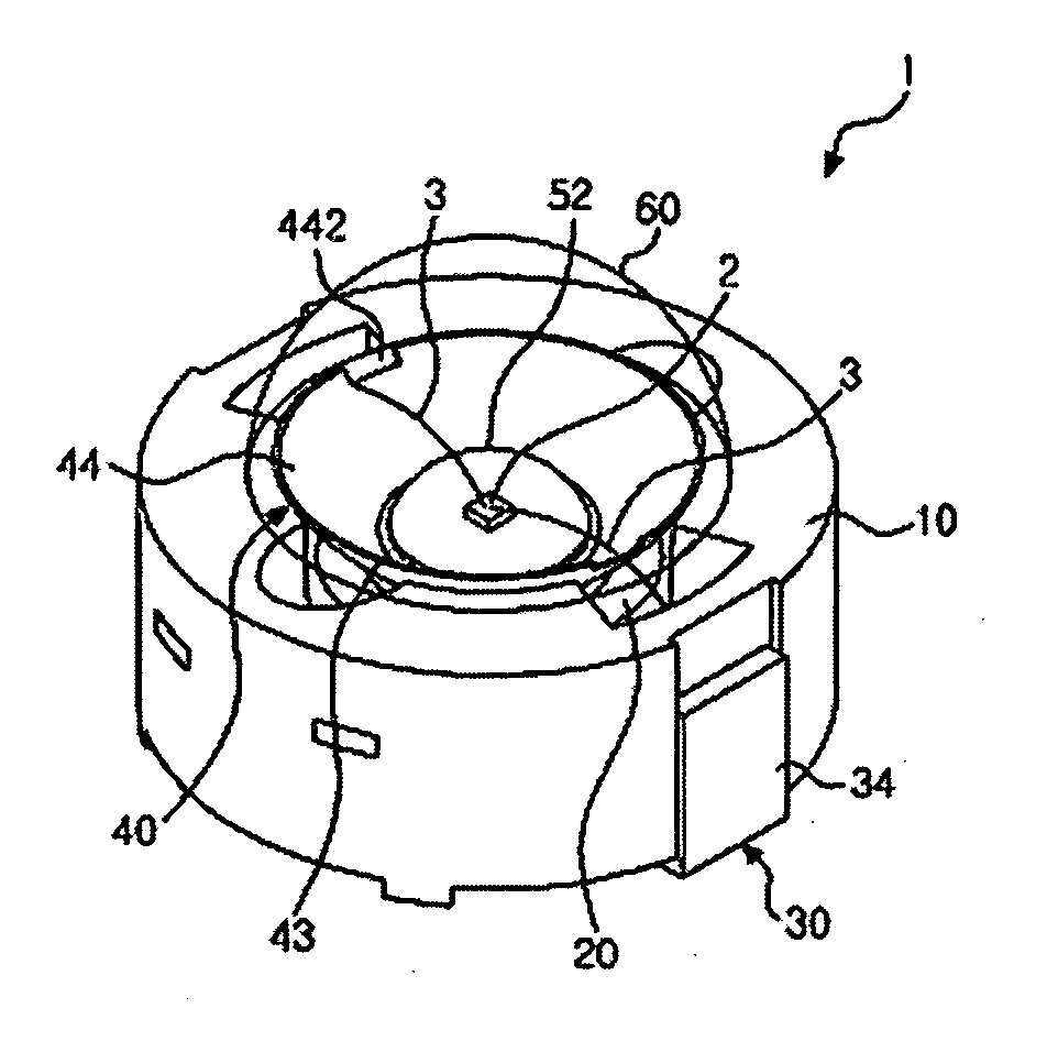
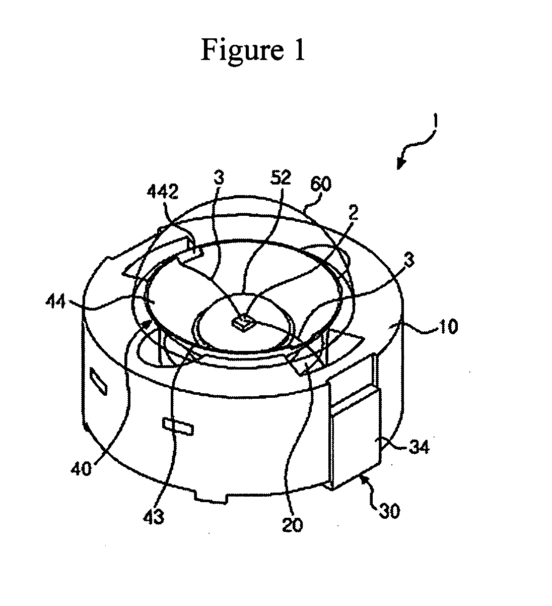
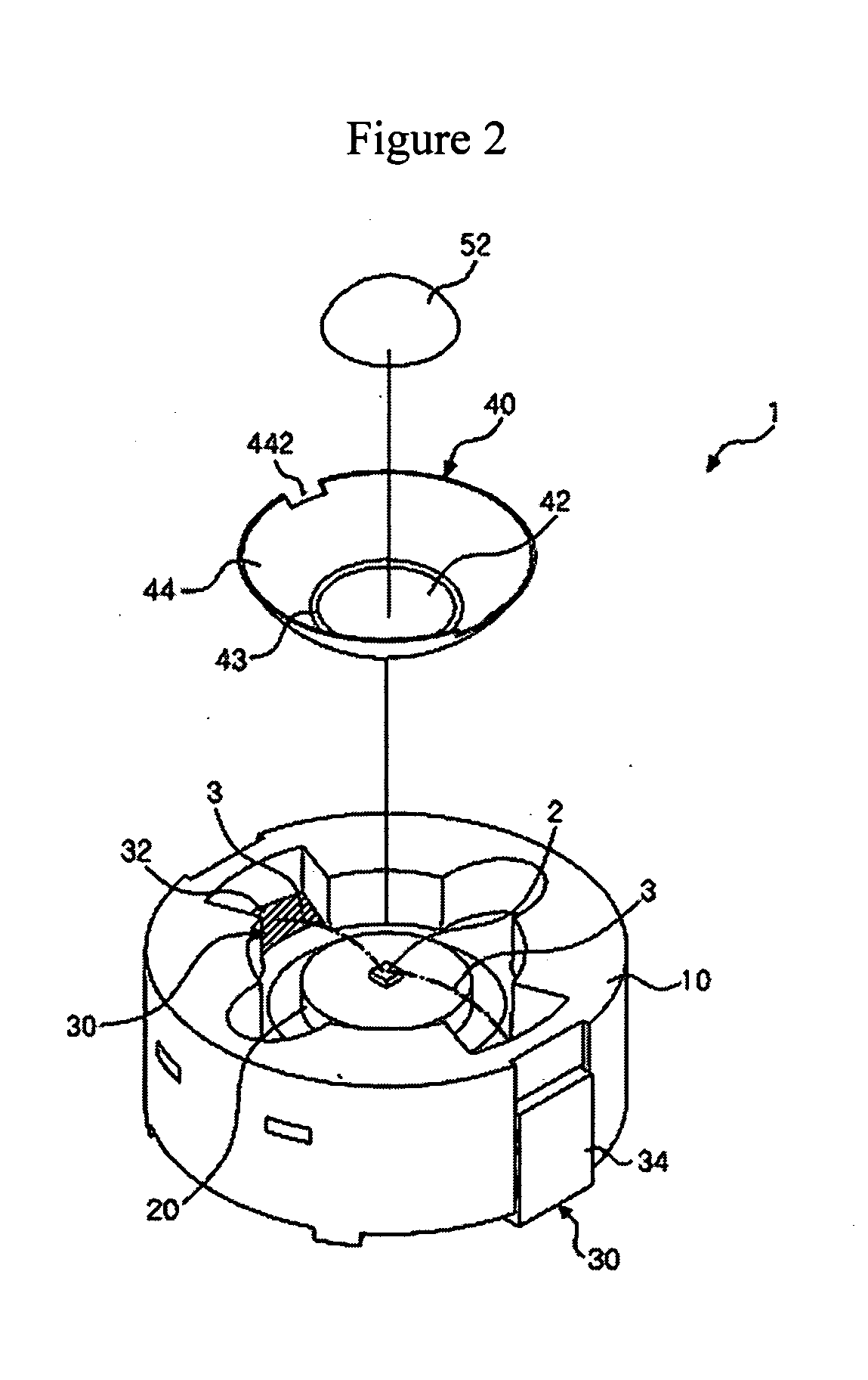
[0039]FIG. 1 is a perspective view generally showing an LED package according to an embodiment of the present invention, FIG. 2 is a partially exploded perspective view showing the LED package according to the embodiment of the present invention with a molding lens removed, and FIG. 3 is a sectional view showing the LED package shown in FIG. 1.

[0040]Referring to FIGS. 1 to 3, an LED package 1 according to the present invention includes a package body 10 having an inner space, in which an LED chip 2 is mounted and which is open upwards in a light emission direction. The package body 10 may be formed by molding and sintering ceramic or by injection molding plastic resin. A heat sink 20, which is conventionally called a heat transfer ‘slug’, is mounted to be inserted into the inner space of the package body 10. At this time, the heat sink may be replaced with a heat pipe structure.

[0041]Further, a lead frame 30 is mounted to the package body 10. Inner leads 32 (shown in FIGS. 2 and 3) ...

embodiment 2

[0060]Hereinafter, an LED package according to another embodiment of the present invention will be described with reference to FIGS. 6 to 10. Like reference numerals will be assigned to represent the constitutional elements which perform the same functions as described above.

[0061]Referring to FIGS. 6 to 9, an LED package 1 of this embodiment includes the heat sink 20 as a chip support member, and the dish-shaped reflector 40.

[0062]A protrusion stage 22 having a substantial quadrangular cross section is provided on an upper end of the heat sink 20, and the LED chip 2 is attached and supported to the end surface of the protrusion stage 22. The LED chip 2 is encapsulated by the phosphor resin member 52 formed on and defined by the end surface of the protrusion stage 22. The phosphor resin member 52 is formed by curing liquefied resin (hereinafter, liquefied phosphor resin) containing a powder-type phosphor material, which is dotted on the end surface of the protrusion stage 22. At thi...

embodiment 3

[0077]Hereinafter, an LED package according to another embodiment of the present invention will be described with reference to FIGS. 11 to 14. Like reference numerals will be assigned to represent the constitutional elements which perform the same functions as described above.

[0078]Referring to FIGS. 11 to 14, the LED package of this embodiment includes the heat sink 20 and a cavity 23, wherein the heat sink 20 is installed to the package body 10 and the cavity 23 is formed on an upper portion of the heat sink 20.

[0079]A bottom of the package body 10 is configured to be closed by a lower portion of the heat sink 20 while an upper portion of the package body 10 is open for providing the light emission and forming the molding lens 60. The upper portion of the heat sink 20 is formed with the cup shaped cavity 23, and a groove 24 is formed on an edge of an inside bottom of the cavity 23. The groove 24 on the bottom of the cavity 23 is generally formed in a ring shape. However, the groov...


PUM


Abstract

The present invention has an object to provide a LED package having a means capable of precisely limiting a region in which a resin containing a phosphor is dotted on a member on which an LED chip is supported. To this end, an LED package according to the present invention comprises a package body having an inner space with an LED chip mounted therein, the inner space being open toward a light emission direction; a chip support member mounted to the inner space of the package body to support the LED chip; a phosphor resin member formed by dotting resin containing a phosphor onto the LED chip; and a region limitation means provided on the chip support member and defining a region in which the phosphor resin member is formed.

Description

CROSS REFERENCE TO RELATED APPLICATIONS[0001]This application is the National Stage of International Application No. PCT / KR2007 / 004727, filed Sep. 27, 2007, and claims priority from and the benefit of Korean Patent Application No. 10-2006-0095653, filed on Sep. 29, 2006, Korean Patent Application No. 10-2006-0095656, filed on Sep. 29, 2006, and Korean Patent Application No. 10-2006-0095657, filed on Sep. 29, 2006, which are all hereby incorporated by reference for all purposes as if fully set forth herein.BACKGROUND OF THE INVENTION[0002]1. Field of the Invention[0003]The present invention relates to a light emitting diode (LED) package, and more specifically, to a LED package having a fence of a phosphor resin member and a manufacturing method thereof[0004]2. Discussion of the Background[0005]Generally, an LED package has a structure in which an LED chip for generating light by p-n junction is mounted on an inner space of a package body. The package body is open in a light emission...

Claims


Application Information

Patent Timeline
IPC IPC(8): H01L33/00H01L33/48H01L33/50H01L33/54H01L33/56H01L33/60H01L33/64
CPCH01L33/483H01L33/508H01L33/54H01L33/56H01L33/60H01L2224/48091H01L33/642H01L2933/0041H01L2924/00014
Inventor KWON, YOU JINSEO, JUNG HUPYO, BYOUNG KICHO, KANG HYUN
Owner SEOUL SEMICONDUCTOR
Why Eureka
Try Eureka