Semiconductor device and method for manufacturing the same

Active Publication Date: 2015-07-02
SEMICON ENERGY LAB CO LTD
View PDF10 Cites 51 Cited by
  • Summary
  • Abstract
  • Description
  • Claims
  • Application Information

AI Technical Summary

Benefits of technology

[0013]According to a structure disclosed in Patent Document 4, a Cu—Mn alloy film is formed over an oxide semiconductor, and then heat treatment is performed on the Cu—Mn alloy film to form an Mn oxide at the joint interface between the oxide semiconductor and the Cu—Mn alloy film. The Mn oxide is formed in such a manner that Mn in the Cu—Mn alloy film diffuses toward the oxide semiconductor and is prefe

Problems solved by technology

However, a Cu film is disadvantageous in that adhesion thereof to a base film is low, dry etching thereof is difficult, and characteristics of a transistor easily deteriorates due to diffusion of Cu from the Cu film into a semiconductor layer of the transistor.
However, in the case where a transistor us

Method used


Image

  • Semiconductor device and method for manufacturing the same
  • Semiconductor device and method for manufacturing the same
  • Semiconductor device and method for manufacturing the same

Examples


embodiment 1

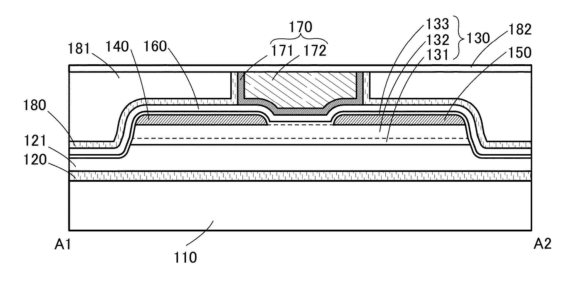
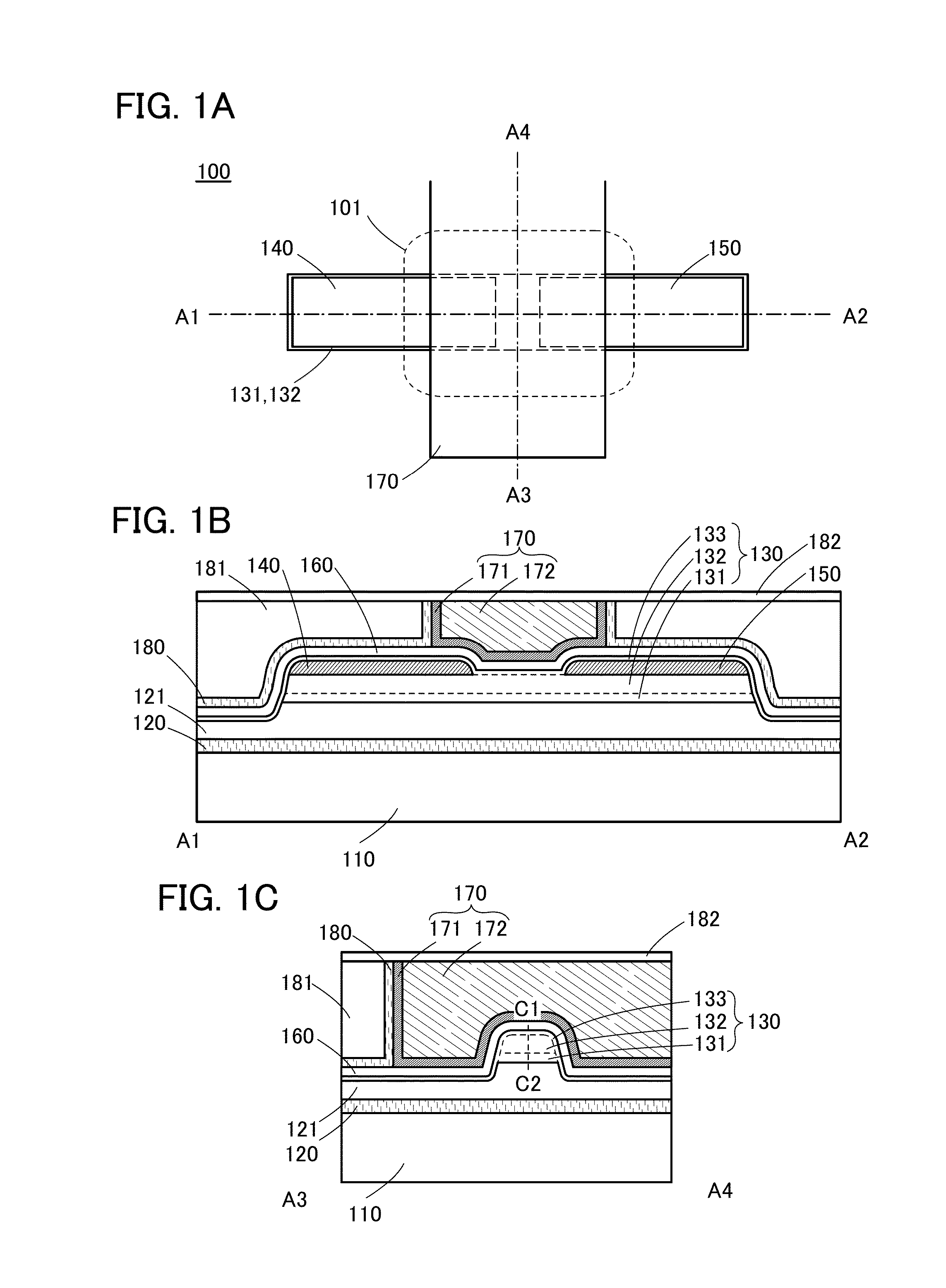
[0081]In this embodiment, a semiconductor device of one embodiment of the present invention will be described with reference to drawings.

[0082]FIG. 1A is a top view of a semiconductor device 100 of one embodiment of the present invention. A cross-sectional view of a transistor 101 in the channel length direction, taken along a dashed line A1-A2 in FIG. 1A, is shown in FIG. 1B. A cross-sectional view of the transistor 101 in the channel width direction, taken along a dashed line A3-A4 in FIG. 1A, is shown in FIG. 1C. Note that in FIG. 1A, some components of the semiconductor device 100 are not illustrated to avoid complexity.

[0083]Note that the channel length refers to, for example, a distance between a source (a source region or a source electrode) and a drain (a drain region or a drain electrode) in a region where a semiconductor (or a portion where a current flows in a semiconductor when a transistor is on) and a gate electrode overlap with each other or a region where a channel i...

embodiment 2

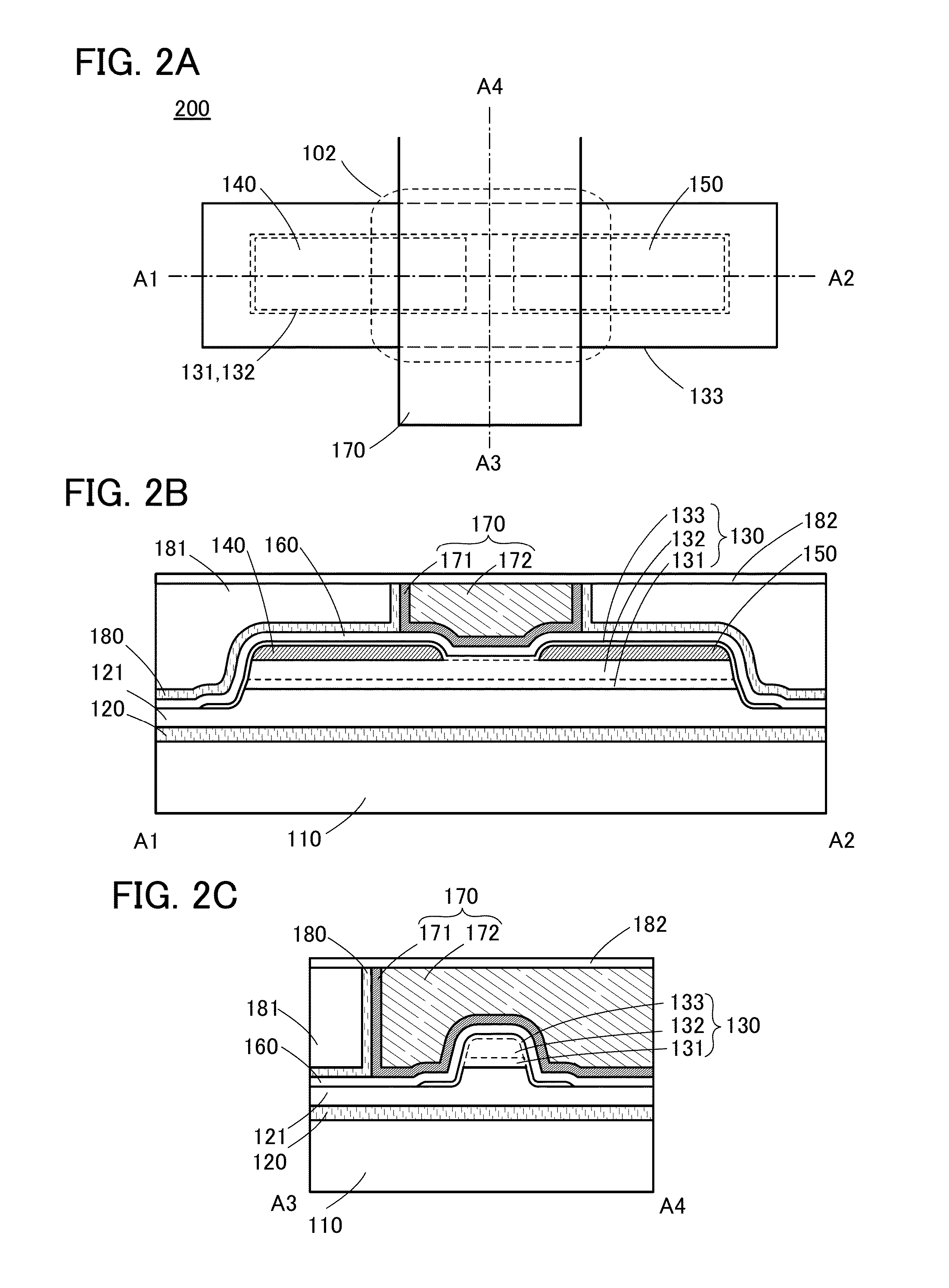
[0205]In this embodiment, a semiconductor device 200 including a transistor 102 of one embodiment of the present invention will be described with reference to FIGS. 2A to 2C.

[0206]FIG. 2A is a top view of the semiconductor device 200 including the transistor 102 of one embodiment of the present invention. The transistor 102 has the same structure as the transistor 101 described in Embodiment 1 except that the shape of the oxide semiconductor 133 is different. Specifically, a side surface of the oxide semiconductor 133 is covered with the gate insulating film 160 in the transistor 102.

[0207]FIG. 2B is a cross-sectional view in the channel length direction, taken along a dashed line A1-A2 in FIG. 2A. FIG. 2C is a cross-sectional view in the channel width direction, taken along a dashed line A3-A4 in FIG. 2A. Note that in FIG. 2A, some components of the semiconductor device 200 are not illustrated to avoid complexity.

[0208]As in the transistor 101, a Cu—X alloy film is preferably used ...

embodiment 3

[0215]In this embodiment, a semiconductor device 300 including a transistor 103 of one embodiment of the present invention will be described with reference to FIGS. 3A to 3C.

[0216]FIG. 3A is a top view of the semiconductor device 300 including the transistor 103 of one embodiment of the present invention. The transistor 103 has the same structure as the transistor 101 described in Embodiment 1 except that the gate insulating film 160 and the oxide semiconductor 133 are formed by patterning with the use of the sacrificial layer 173b as a mask.

[0217]FIG. 3B is a cross-sectional view in the channel length direction, taken along a dashed line A1-A2 in FIG. 3A. FIG. 3C is a cross-sectional view in the channel width direction, taken along a dashed line A3-A4 in FIG. 3A. Note that in FIG. 3A, some components of the semiconductor device 300 are not illustrated to avoid complexity.

[0218]As in the transistor 101, a Cu—X alloy film is preferably used as the conductive film 171 of the transisto...


PUM


Abstract

A novel semiconductor device with a transistor using an oxide semiconductor film, in which a conductive film including Cu is used as a wiring or the like, is provided. The semiconductor device includes a first insulating film, an oxide semiconductor over the first insulating film, a gate electrode overlapping the oxide semiconductor with a gate insulating film positioned therebetween, a second insulating film in contact with a side surface of the gate electrode, and a third insulating film in contact with a top surface of the gate electrode. The gate electrode includes a Cu—X alloy film (X is Mn, Ni, Cr, Fe, Co, Mo, Ta, Ti, Zr, Mg, Ca, or a mixture of two or more of these elements).

Description

BACKGROUND OF THE INVENTION[0001]1. Field of the Invention[0002]The present invention relates to semiconductor devices using oxide semiconductors and methods for manufacturing the semiconductor devices.[0003]Note that one embodiment of the present invention is not limited to the above technical field. The technical field of one embodiment of the invention disclosed in this specification and the like relates to an object, a method, or a manufacturing method. In addition, one embodiment of the present invention relates to a process, a machine, manufacture, or a composition of matter. Specifically, examples of the technical field of one embodiment of the present invention disclosed in this specification include a semiconductor device, a display device, a liquid crystal display device, a light-emitting device, a lighting device, a power storage device, a storage device, a method for driving any of them, and a method for manufacturing any of them.[0004]In this specification and the like,...

Claims


Application Information

Patent Timeline
IPC IPC(8): H01L29/49H01L29/66H01L29/786
CPCH01L29/4958H01L29/66969H01L29/7869H01L29/78648H01L29/78696H01L27/1225
Inventor MIYAIRI, HIDEKAZU
Owner SEMICON ENERGY LAB CO LTD
Why Eureka
Try Eureka