Method for manufacturing nitride semiconductor device

a semiconductor device and nitride technology, applied in the field of manufacturing a semiconductor device, can solve the problems of nitrogen loss, inability to obtain a p-type layer with a high carrier concentration, etc., and achieve the effects of low specific resistance, high carrier concentration, and easy dispersion

Inactive Publication Date: 2009-03-12
ROHM CO LTD
View PDF1 Cites 7 Cited by
  • Summary
  • Abstract
  • Description
  • Claims
  • Application Information

AI Technical Summary

Benefits of technology

[0013]According to the present invention, since a bonding between the acceptor, for example Mg, doped into the nitride semiconductor layer and H is separated off by irradiating a laser beam and a heat treatment is carried out at a low temperature of 300 to 400° C. thereafter, the separated H can be easily dispersed out of the nitride semiconductor layer. As a result, nitrogen vacancies caused by decomposing of nitrogen from a surface of the nitride semiconductor layer are not formed because it is not necessary to carry out a heat treatment at a high temperature for an extended time in order to activate the acceptor only by an annealing treatment. Thereby, since activation of, for example, Mg of an acceptor can be carried out surely, because of no decrease of a hole concentration by nitrogen vacancies, a p-type layer with remarkably high carrier concentration and with a low specific resistance can be obtained, and, as a result, the nitride semiconductor device can be obtained such as semiconductor light emitting device with high performance or the like.

Problems solved by technology

However, when the annealing treatment at a high temperature of 400° C. or more is carried out in order to separate off a bonding between the Mg and H, and to disperse the H, nitrogen in a surface of the nitride semiconductor layer becomes apt to be dispersed and a phenomenon of nitrogen loss occurs.
When nitrogen loss occurs, a nitrogen vacancy is formed, the nitrogen vacancy acts as a donor and lowers a concentration of holes, and finally there arises a problem such that the p-type layer with a high carrier concentration can not be obtained.

Method used


Image

  • Method for manufacturing nitride semiconductor device
  • Method for manufacturing nitride semiconductor device
  • Method for manufacturing nitride semiconductor device

Examples


Embodiment Construction

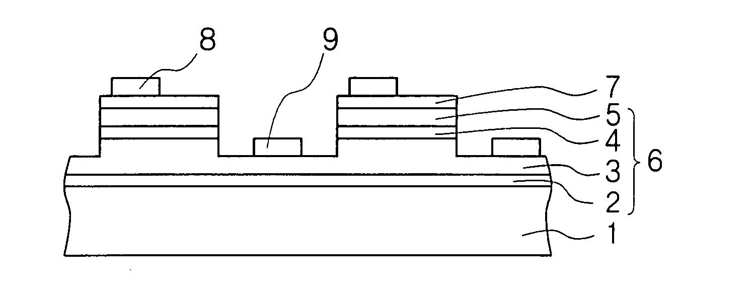
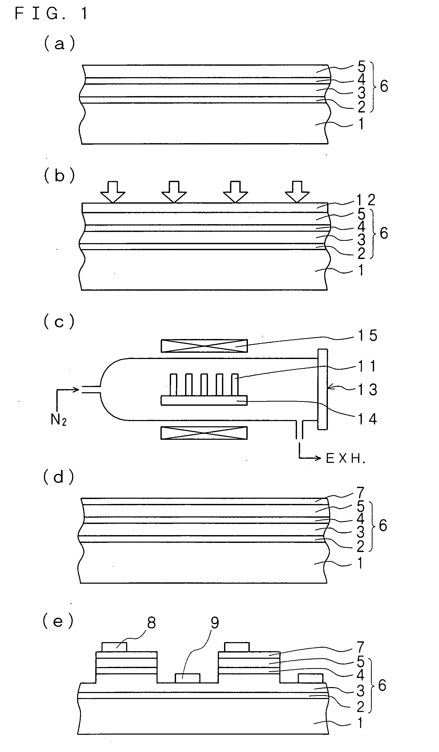
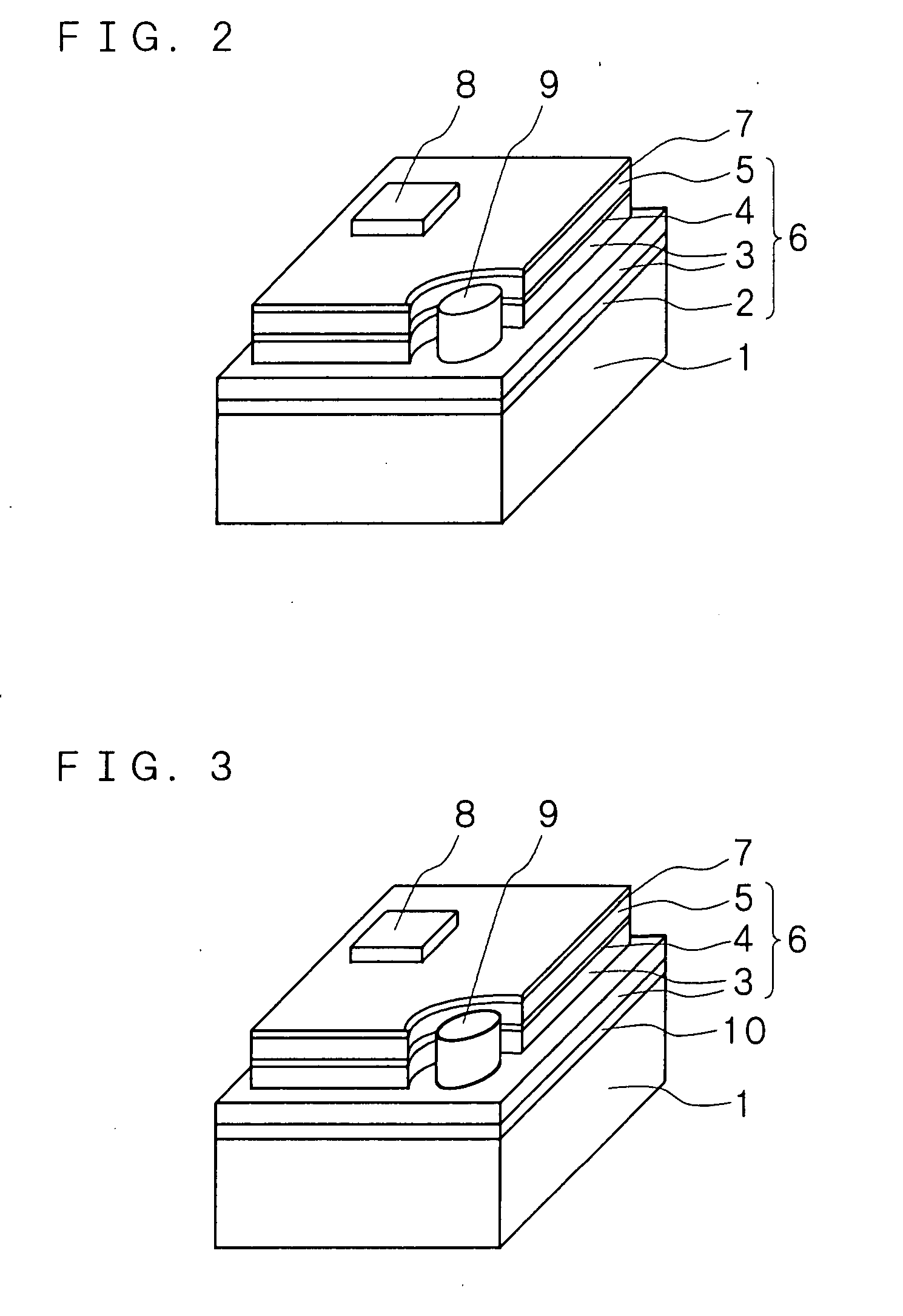
[0029]An explanation will be given below of a method for manufacturing a nitride semiconductor device according to the present invention in reference to the drawings. In case that a nitride semiconductor device is formed which has a p-type nitride semiconductor layer formed at a surface side of nitride semiconductor layers grown on a substrate by MOCVD method, the method for manufacturing a nitride semiconductor device according to the present invention includes the steps of: irradiating a laser beam having energy capable of separating off a bonding between Mg which is an acceptor and H, on a nitride semiconductor layer doped with the acceptor to make the p-type layer activate, thereby separating off the bonding between the Mg and the H; and dispersing the H separated off out of the nitride semiconductor layer by carrying out a heat treatment at a temperature of 300 to 400° C., thereby activating the acceptor.

[0030]Concretely, as an explanatory cross-sectional view of a manufacturin...


PUM


Abstract

There is provided a method for manufacturing a nitride semiconductor device which has a p-type nitride semiconductor layer having a high carrier concentration (low resistance) by activating an acceptor without raising a problem of forming nitrogen vacancies which are generated when a high temperature annealing is carried out over an extended time. A semiconductor lamination portion (6) made of nitride semiconductor is formed on a substrate (1) so as to form a light emitting layer, and irradiated by a laser beam having a wavelength λ of λ=h*c/E or less (E is energy capable of separating off the bonding between Mg and H) from the front surface side of the semiconductor lamination portion. Then, a heat treatment is carried out at a temperature of 300 to 400° C. And, similarly to a process for normal nitride semiconductor LED, a light transmitting conductive layer (7) is provided, an n-side electrode (9) is formed on an n-type layer (3) exposed by removing a part of the semiconductor lamination portion by etching, and a p-side electrode (8) is formed on a surface of the light transmitting conductive layer, thereby a LED is obtained.

Description

FIELD OF THE INVENTION[0001]The present invention relates to a method for manufacturing a semiconductor device using a p-type nitride semiconductor crystal layer such as a light emitting device like a light emitting diode (LED), a laser diode or the like, and a transistor device like a HEMT or the like, using nitride semiconductor. More particularly, the present invention relates to a method for a nitride semiconductor device in which an acceptor can be surely activated and a p-type layer of a low resistance can be obtained, without bringing on a bad effect of nitrogen loss caused by carrying out a heat treatment at a high temperature in order to activate an acceptor in the p-type nitride semiconductor layer.BACKGROUND OF THE INVENTION[0002]Nitride semiconductor light emitting devices such as a blue light emitting diode (LED), a laser diode or the like, using nitride semiconductor have been lately in practical use. The semiconductor light emitting device using nitride semiconductor ...

Claims


Application Information

Patent Timeline
Patent Type & Authority Applications(United States)
IPC IPC(8): H01L33/00H01L21/338H01L33/12H01L33/32
CPCH01L21/0237H01L21/0242H01L21/02458H01L21/02507H01L21/0254H01L33/305H01L21/02579H01L21/0262H01L21/268H01L29/66462H01L33/0095H01L21/02576
Inventor NAKAHARA, KEN
Owner ROHM CO LTD
Why Eureka
Try Eureka