

Static electricity protection circuit, semiconductor device, and electronic apparatus
a technology of static electricity protection circuit and semiconductor device, which is applied in the direction of semiconductor devices, diodes, electrical devices, etc., can solve the problems of increasing the risk of breaking the component element, the heat generation due to the breakdown current is greater than the heat radiation,
- Summary
- Abstract
- Description
- Claims
- Application Information
AI Technical Summary
Benefits of technology
Problems solved by technology
Method used
Image

Examples
example 1
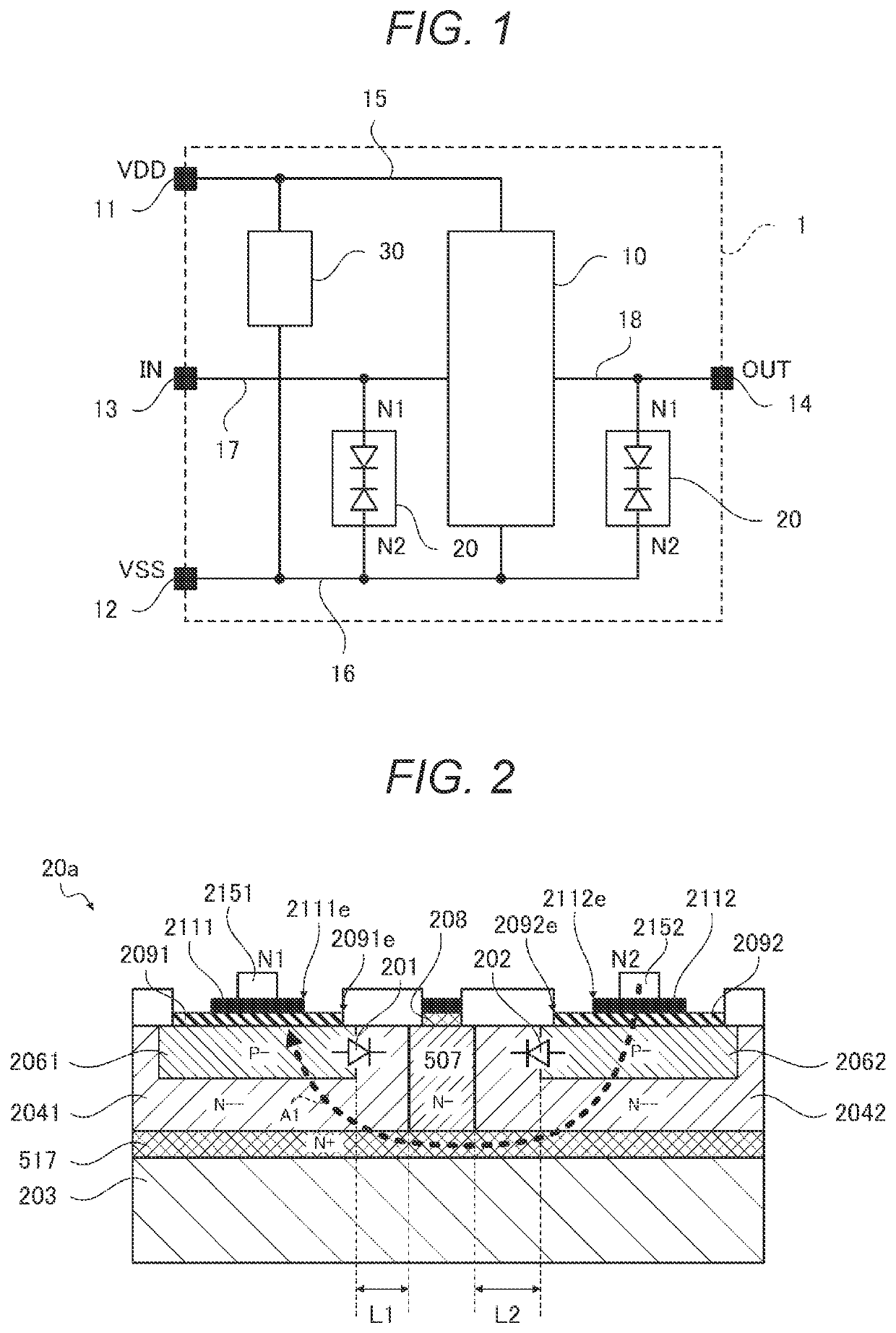
[0047]A static electricity protection circuit 20a as Example 1 of the static electricity protection circuit 20 shown in FIG. 1 will now be described with reference to FIG. 2.
[0048]The static electricity protection circuit 20a has the N-type N−-semiconductor region 2041 and the N-type N−-semiconductor region 2042, the N− common impurity region 507 having a higher N-type carrier concentration than the N−-semiconductor region 2041 and the N−-semiconductor region 2042, the N+ embedded region 517 having a higher N− type carrier concentration than the N− common impurity region 507, and the P-type P− impurity region 2061 and the P-type P− impurity region 2062.
[0049]Also, the static electricity protection circuit 20a has the electrode 2151, the impurity region semiconductor layer 2091 having a higher P-type carrier concentration than the P− impurity region 2061, and the metal compound layer 2111, and also has the electrode 2152, the impurity region semiconductor layer 2092 having a higher P...
example 2
[0079]Example 2 will now be described with reference to FIG. 7.
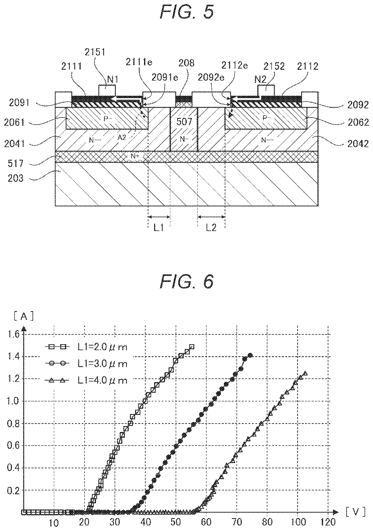
[0080]In Example 1, the positive hold voltage and the negative hold voltage can be made different from each other by making the distance L1 and the distance L2 different from each other. However, there is a case where the hold voltage may become excessively high, for example, even when the distance L1 contributing to one hold voltage is 0 μm. In this case, the electrostatic withstand voltage of the internal circuit 10 needs to be designed to be higher than the hold voltage. To cope with this, in a static electricity protection circuit 20b according to this example, the impurity region semiconductor layer 2091 is spaced apart from the common impurity region semiconductor layer 208 in the upward direction from the P− impurity region 2061 and the N− common impurity region 507 and extends over the N− common impurity region 507 from the P− impurity region 2061, and is coupled to the P− impurity region 2061 and the N− common i...
PUM
| Property | Measurement | Unit |
|---|---|---|
| hold voltage | aaaaa | aaaaa |
| hold voltage | aaaaa | aaaaa |
| hold voltage | aaaaa | aaaaa |
Abstract
Description
Claims
Application Information