
Semiconductor memory device

Active Publication Date: 2010-03-25
KIOXIA CORP
View PDF4 Cites 84 Cited by
  • Summary
  • Abstract
  • Description
  • Claims
  • Application Information

AI Technical Summary

Problems solved by technology

However, access by data reading or data writing is performed irregularly.
This causes increase of power consumption.

Method used


Image

  • Semiconductor memory device
  • Semiconductor memory device
  • Semiconductor memory device

Examples


first embodiment

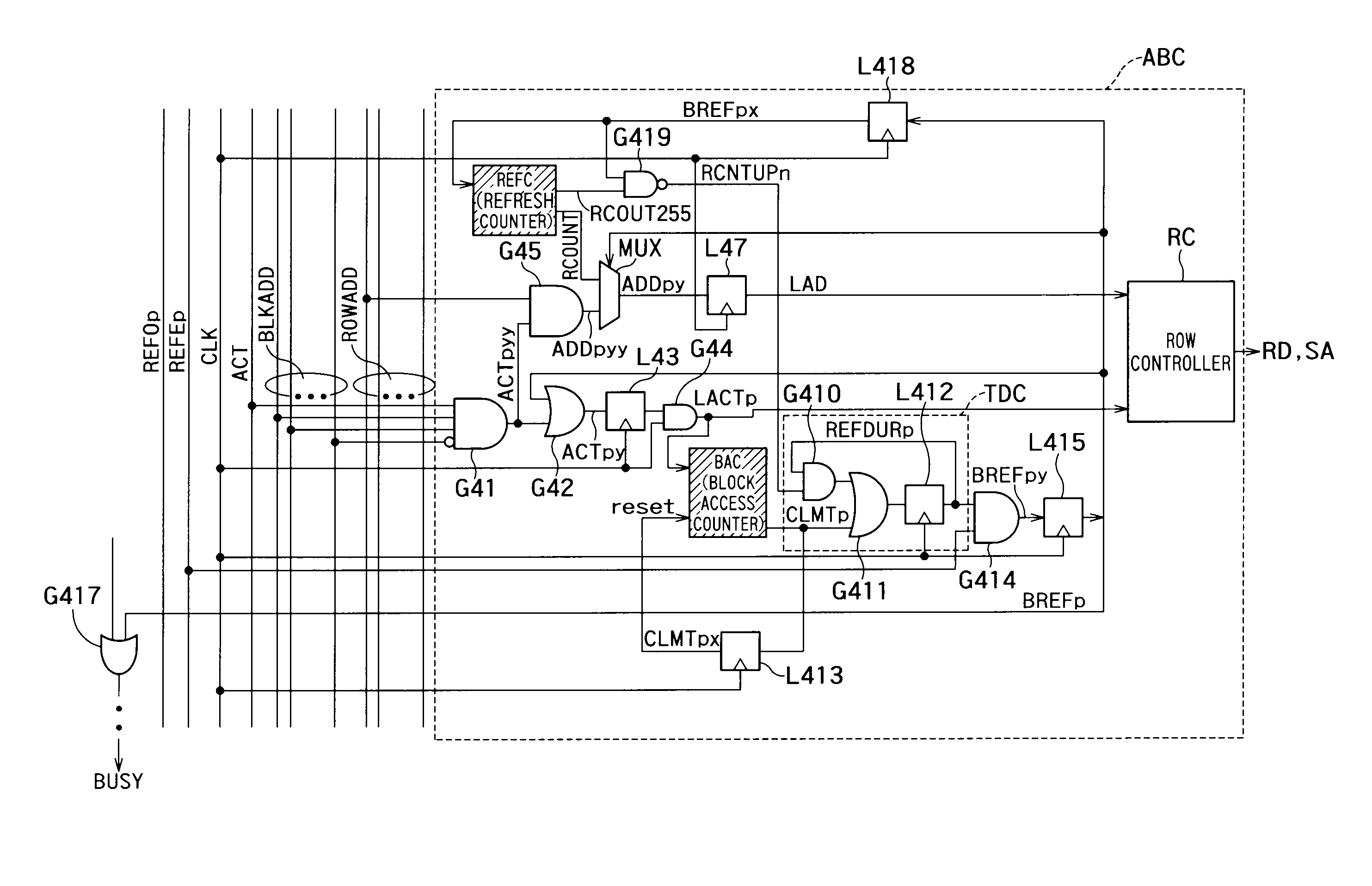
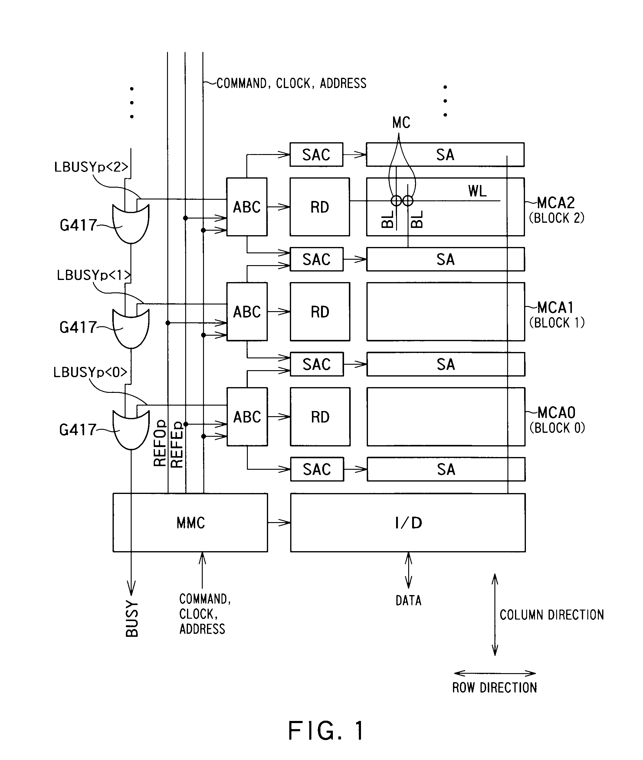
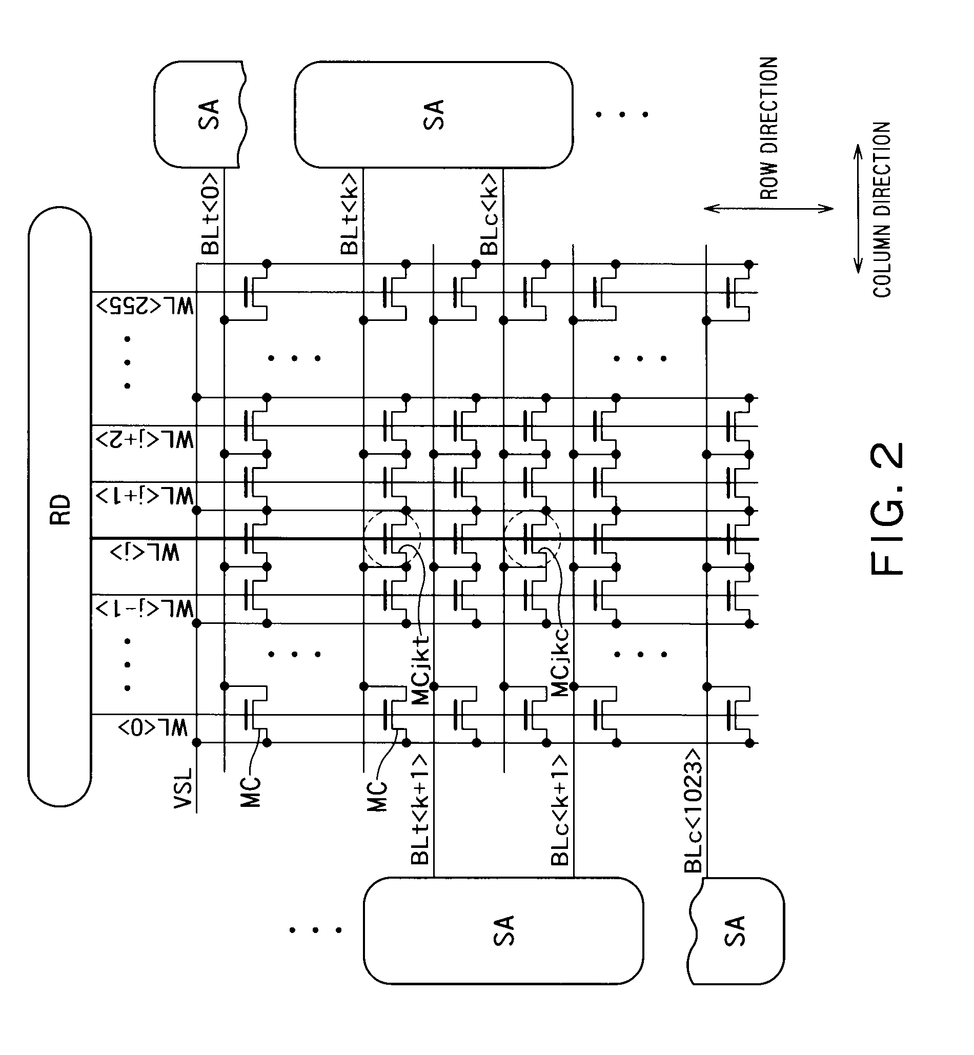
[0020]FIG. 1 is a block diagram showing a configuration of an FBC (Floating Body Cell) memory according to a first embodiment of the present invention. An FBC memory is configured by a FET (Field Effect Transistor) comprising floating bodies on a SOI (Silicon On Insulator) substrate and stores data “1” and / or data “0” in each memory cell by the number of carriers accumulated in the body. The FBC memory includes plural bit lines BL, plural word lines WL, and memory cell arrays as memory cell blocks. FIG. 1 shows three memory cell arrays MCA0 to MCA2 out of all memory cell arrays. The bit lines BL and the word lines WL are orthogonal with each other. Plural memory cells MC are provided corresponding to intersections between the bit lines BL and the word lines WL. Plural memory cells MC constitute the memory cell arrays MCA0 to MCA2 two dimensionally arranged in a matrix shape. The memory cell arrays MCA0 to MCA2 are units of a data read operation or a data write operation. Therefore, ...

second embodiment

[0081]FIG. 8 is a block diagram showing a configuration of the array block controller ABC according to a second embodiment of the present invention. The second embodiment is different from the first embodiment in that the AND gate G414 is not provided in the second embodiment. Other configurations of the second embodiment can be similar to those of the first embodiment. Therefore, in the second embodiment, when the number of times of access reaches a predetermined value, the word lines WL within this memory cell array MCA are continuously selected and a refresh operation is performed, without depending on the signals REFEp and REFOp. In this case, the word lines WL are continuously driven in the order of addresses by matching a continuous series of clock signals CLK, and the memory cells MC connected to the word lines WL are refreshed.

[0082]FIG. 9 is a timing diagram showing a detailed example of an operation of the FBC memory according to the second embodiment. An interval between ...


PUM


Abstract

A memory may includes: word lines; bit lines; memory array blocks including memory cells, each memory array block being a unit of a data read operation or a data write operation; a row decoder configured to selectively drive the word lines; sense amplifiers configured to detect data; and an access counter provided for each memory cell block, the access counter counting the number of times of accessing the memory array blocks in order to read data or write data, and activating a refresh request signal when the number of times of access reaches a predetermined number of times, wherein during an activation period of the refresh request signal of the access counter, the row decoder periodically and sequentially activates the word lines of the memory array blocks corresponding to the access counter, and the sense amplifier performs a refresh operation of the memory cells connected to the activated word lines.

Description

CROSS-REFERENCE TO RELATED APPLICATION[0001]This application is based upon and claims the benefit of priority from the prior Japanese Patent Applications No. 2008-244454, filed on Sep. 24, 2008, the entire contents of which are incorporated herein by reference.BACKGROUND OF THE INVENTION[0002]1. Field of the Invention[0003]The present invention related to a semiconductor memory device.[0004]2. Related Art[0005]Regardless of whether a memory is a volatile memory or a nonvolatile memory, disturbance occurs in data of unselected memory cells at a data reading time or at a data writing time. For example, at the time of detecting data of a selected memory cell connected to a selected word line, a potential of a bit line connected to a sense amplifier is also applied to unselected memory cells connected to unselected word lines. In this case, data stored in the unselected memory cells is disturbed by the potential of the bit line. The disturbance is a phenomenon of degrading data stored i...

Claims


Application Information

Patent Timeline
IPC IPC(8): G11C7/00G11C8/00
CPCG11C8/04G11C11/406G11C2211/4067G11C2211/4016G11C11/40615
Inventor FUKUDA, RYOWATANABE, YOHJI
Owner KIOXIA CORP
Features
  • Generate Ideas
  • Intellectual Property
  • Life Sciences
  • Materials
  • Tech Scout
  • Unparalleled Data Quality
  • Higher Quality Content
  • 60% Fewer Hallucinations
Learn More