eFuse and Resistor Structures and Method for Forming Same in Active Region

a resistor and active region technology, applied in semiconductor devices, semiconductor/solid-state device details, diodes, etc., can solve the problems of less polysilicon available for passive devices, reduced polysilicon gate height, and difficult to efficiently form passive devices from very thin polysilicon layers

Inactive Publication Date: 2010-04-01
IBM CORP +1
View PDF8 Cites 26 Cited by
  • Summary
  • Abstract
  • Description
  • Claims
  • Application Information

AI Technical Summary

Problems solved by technology

However, as semiconductor devices are scaled down, the height of the polysilicon gate is reduced in order to obtain better patterning resolution, which means that there is less polysilicon available for use in forming the passive devices.
This problem is exacerbated with newer process technologies which form metal gate electrodes over high-k dielectric layers using very thin polysilicon layers, making it even more difficult to efficiently form passive devices from the very thin polysilicon layers.
For example, the thickness variation in thin polysilicon layers creates design tolerance problems for resistor applications.
And with eFuse applications, th

Method used


Image

  • eFuse and Resistor Structures and Method for Forming Same in Active Region
  • eFuse and Resistor Structures and Method for Forming Same in Active Region
  • eFuse and Resistor Structures and Method for Forming Same in Active Region

Examples


Embodiment Construction

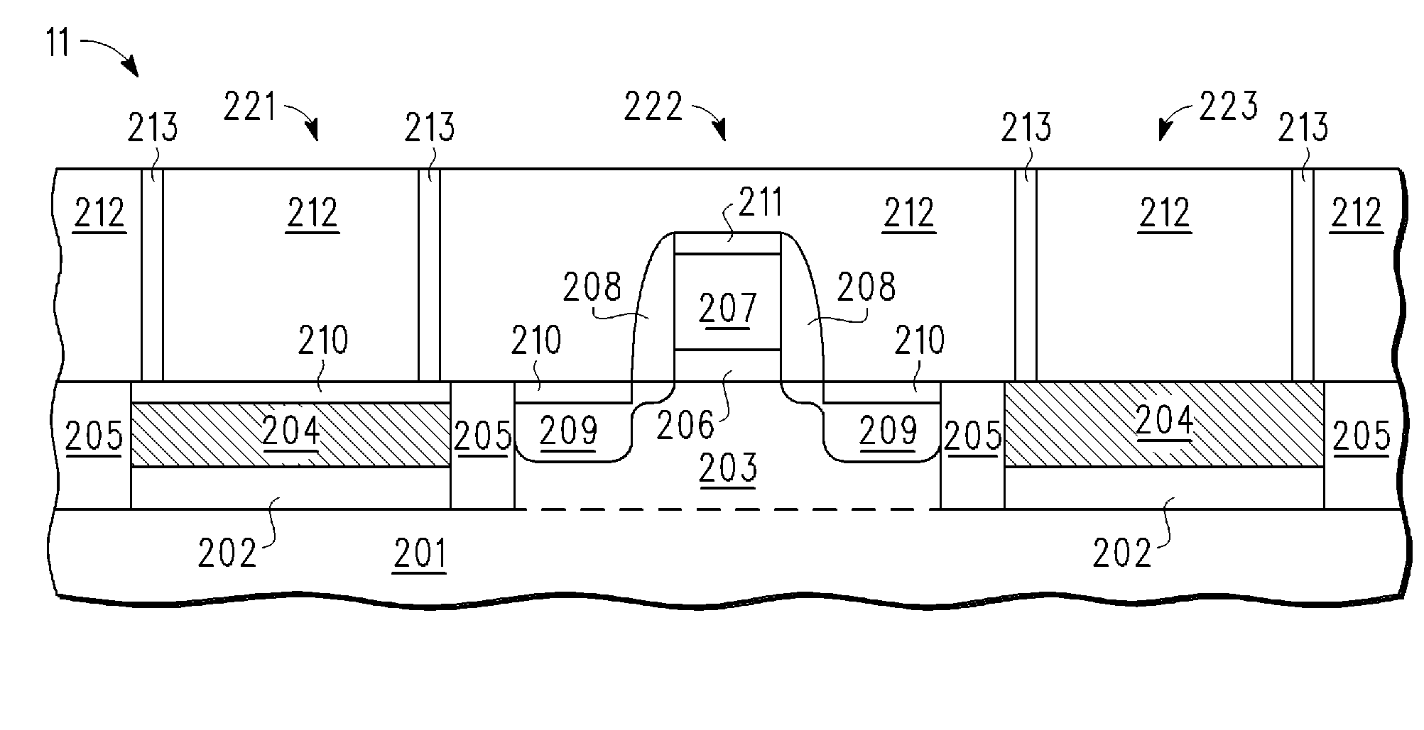
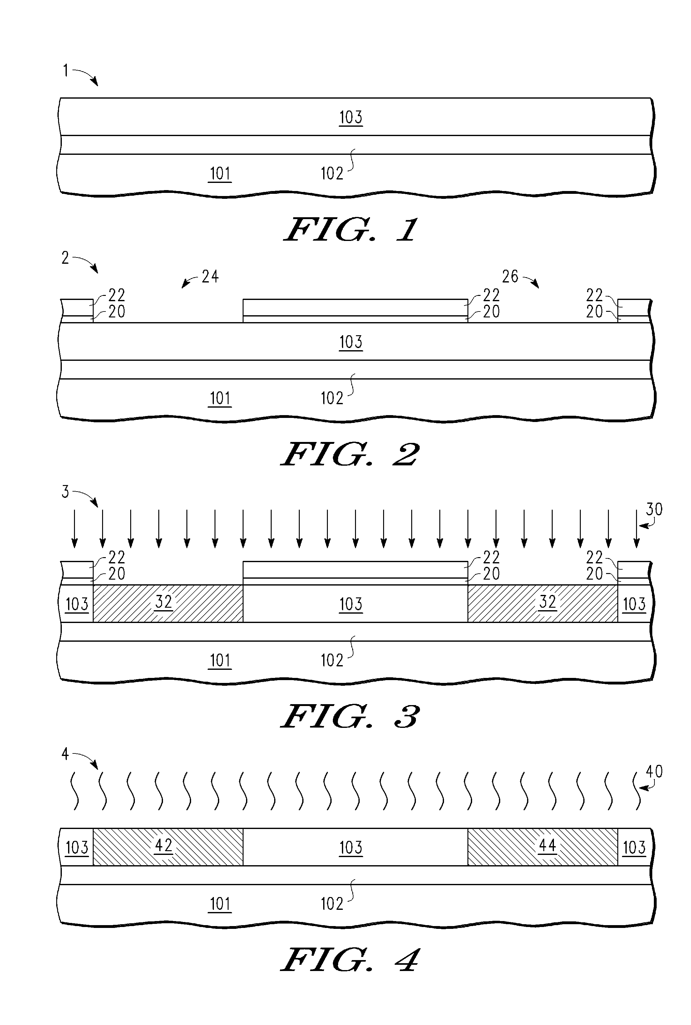
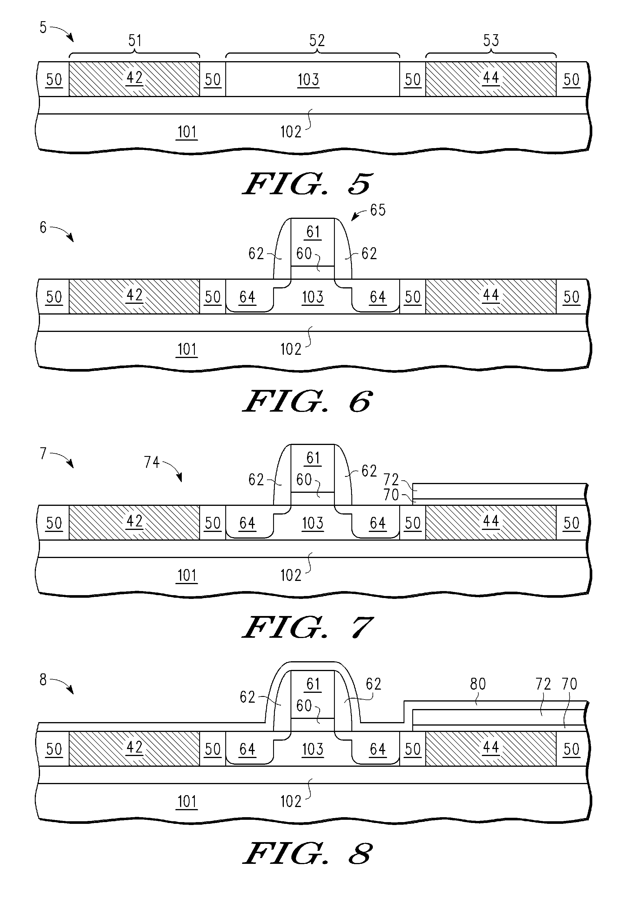
[0020]A semiconductor fabrication process and resulting integrated circuit are described for manufacturing passive devices, such as fuse, eFuse or resistor structures, in an active substrate region of a integrated circuit device by using heavy ion implantation and anneal processes to selectively form amorphous or polycrystalline regions in a monocrystalline active layer, while retaining the single crystalline regions in the active layer for use in forming active devices, such as NMOS and / or PMOS transistors. For example, the crystalline structure of a monocrystalline silicon layer can be changed to have a polycrystalline structure by selectively implanting heavy ion species (e.g., Xe, Ge, Ar, In, Sb, As, P, BF2, Si, and / or other amorphizing ions) into the monocrystalline silicon layer and then annealing the implanted region while other active device areas are protected to maintain the original single crystalline structure. Selected embodiments of the present invention may use patter...


PUM


Abstract

A semiconductor fabrication process and apparatus are provided for forming passive devices, such as a fuse (93) or resistor (95), in an active substrate region (103) by using heavy ion implantation (30) and annealing (40) to selectively form polycrystalline structures (42, 44) from a monocrystalline active layer (103), while retaining the single crystalline regions in the active layer (103) for use in forming active devices, such as NMOS and/or PMOS transistors (94). As disclosed, fuse structures (93) may be fabricated by forming silicide (90) in an upper region of the polycrystalline structure (42), while resistor structures (95) may be simultaneously formed from polycrystalline structure (44) which is selectively masked during silicide formation.

Description

BACKGROUND OF THE INVENTION[0001]1. Field of the Invention[0002]The present invention is directed in general to the field of semiconductor fabrication and integrated circuits. In one aspect, the present invention relates to eFuse and resistor structures fabricated in an active region layer.[0003]2. Description of the Related Art[0004]Semiconductor devices have conventionally been fabricated by forming active devices (such as NMOS and PMOS transistors) over an active region of the semiconductor substrate by patterning polysilicon layers over a single crystal substrate to defined gate electrodes, and then implanting device features (e.g., source / drain regions) around the gate electrodes. With such conventionally formed devices, passive devices (such as capacitors or resistors) are separately formed over a non-active region, such as a field oxide region, by depositing a polysilicon layer over the field oxide which is then patterned and doped as needed to obtain the desired characterist...

Claims


Application Information

Patent Timeline
IPC IPC(8): H01L27/092H01L21/8234H01L21/44
CPCH01L21/84H01L23/5228H01L28/20H01L27/0629H01L27/1203H01L23/5256H01L2924/0002H01L2924/00
Inventor MIN, BYOUNG W.CHAKRAVARTI, SATYA N.
Owner IBM CORP
Why Eureka
Try Eureka