
Eureka
For R&D, Eureka makes reading and utilizing patents & technical documents easy.
Eureka AIR
Designed for self-driven R&D workflows. Generate viable solutions, solve complex R&D challenges, empower your innovation with AI.

Eureka Materials
Designed for material experts only. Revolutionize your material R&D, from search, analyze, to developing new materials.

TechResearch
Generate reliable direction feasibility study reports for your R&D in just a few steps.

TechSeek
Discover and master advanced knowledge NOW. Basics, ideas, possibilities, all at once.

TechMind
As an expert in R&D Theories, TechMind can generates customized viable solutions instantly.

TechRisk
Analyze your overall solution with one click, know your potential R&D risks in advance.

TechMonitor
Get weekly tech updates, stay abreast of the latest tech innovations and key insights.
Circuit testing apparatus and system
- Summary
- Abstract
- Description
- Claims
- Application Information
AI Technical Summary
Benefits of technology
Problems solved by technology
Method used
Image

Examples
first example embodiment
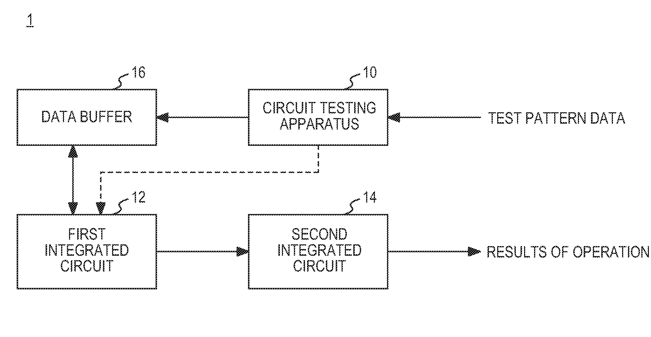
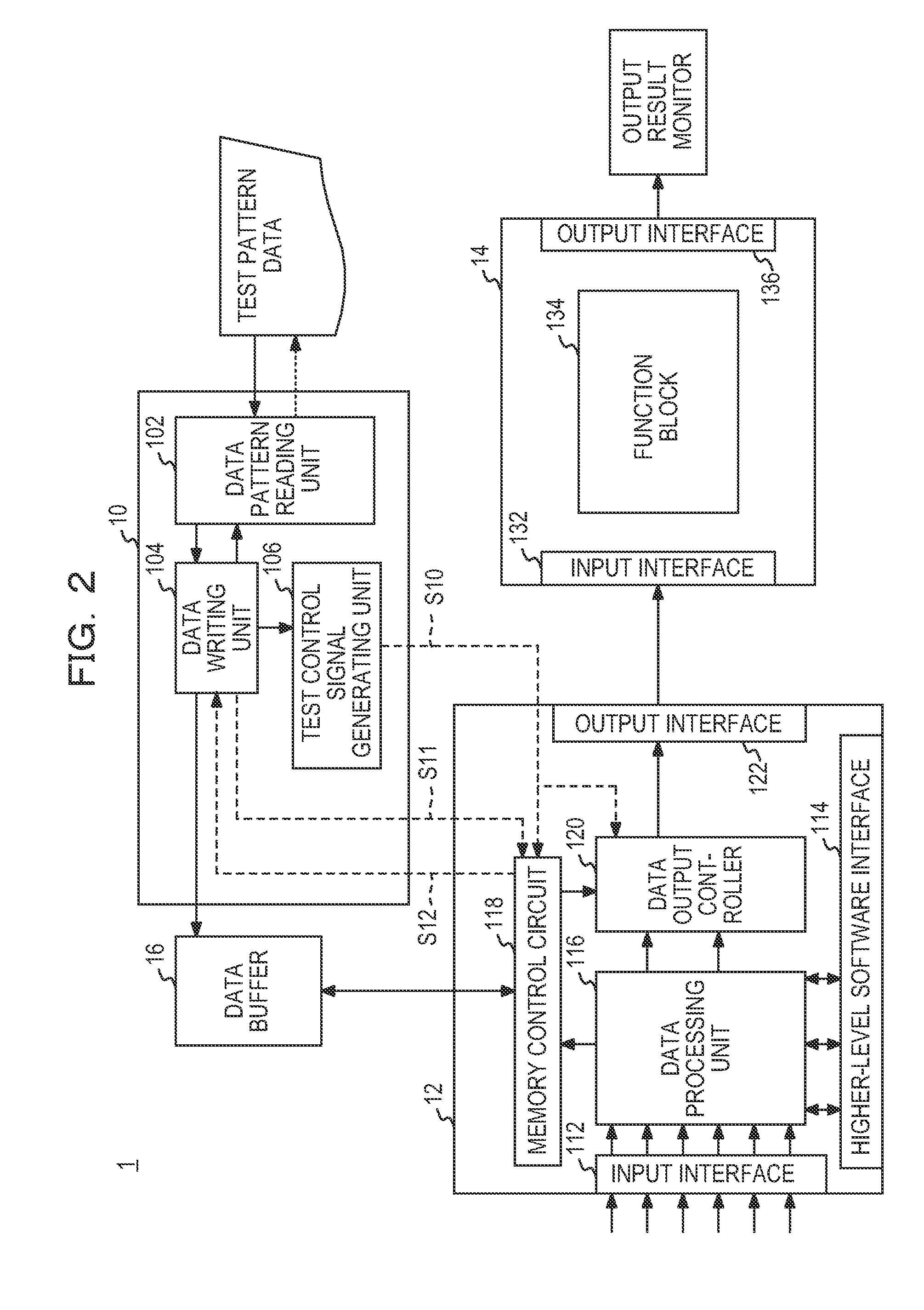
[0017]FIG. 1 illustrates a configuration of a circuit testing system according to a first example embodiment.
[0018]The circuit testing system 1 in FIG. 1 includes a circuit testing apparatus 10, a first integrated circuit 12, a second integrated circuit 14, and an external data buffer 16 of the first integrated circuit 12. The first and second integrated circuits 12 and 14 may implement the same function or different functions.
[0019]Test pattern data used for testing the second integrated circuit 14 is input from an information processor such as a personal computer (PC) or a simple signal generator to the circuit testing apparatus 10. The apparatus that generates the test pattern data may be configured to generate a basic fixed pattern or to generate an arbitrary data pattern by using an FPGA (Field Programmable Gate Array). Alternatively, the test pattern generating apparatus may be configured to dump a buffer pattern from simulation data obtained by a simulation such as an RTL (Re...
second example embodiment
[0033]With the miniaturization of LSIs, the development costs of the LSIs have increased in these years and the manufacturing costs of masks and the like have become very expensive. Against this backdrop, an approach is going mainstream in which a functional verification model (emulation / prototyping circuit) is developed first by using an FPGA or the like and then an actual LSI is developed, with the aims of reducing the remake rate of LSIs and speeding up functional verification of the LSIs. FIG. 3 illustrates a second example embodiment, which is a circuit testing system in which a functional verification model is introduced in a circuit testing apparatus.
[0034]The circuit testing system 2 in FIG. 3 has the same configuration as the circuit testing system according to the first example embodiment illustrated in FIG. 2, except that a functional verification model is introduced in a circuit testing apparatus 20. Therefore the description of the components of the circuit testing syst...
third example embodiment
[0048]FIG. 5 illustrates a configuration of a circuit testing system according to a third example embodiment.
[0049]The circuit testing system 3 in FIG. 5 includes test signal generating units 30a to 30d, a first integrated circuit 32, a second integrated circuit 34, and output result monitors 36a and 36b.
[0050]Each of the test signal generating units 30a to 30d includes a circuit testing apparatus 10 used in the circuit testing system according to the first example embodiment illustrated in FIG. 2 or a circuit testing apparatus 20 according to the second example embodiment illustrated in FIG. 4, and external data buffers for the integrated circuits 32 and 34.
[0051]The first integrated circuit 32 may be an LSI used in a communication apparatus, for example, and includes an ingress processing unit 310 that performs ingress processing for data from a user to a network and an egress processing unit 320 that performs egress processing for data in the opposite direction. The first integr...
PUM
 Abstract
Description
Claims
Application Information
 - R&D Engineer
- R&D Manager
- IP Professional
- Industry Leading Data Capabilities
- Powerful AI technology
- Patent DNA Extraction
Browse by: Latest US Patents, China's latest patents, Technical Efficacy Thesaurus, Application Domain, Technology Topic, Popular Technical Reports.
© 2024 PatSnap. All rights reserved.Legal|Privacy policy|Modern Slavery Act Transparency Statement|Sitemap|About US| Contact US: help@patsnap.com