Semiconductor laser device and display

Inactive Publication Date: 2010-04-01
SANYO ELECTRIC CO LTD
View PDF4 Cites 8 Cited by
  • Summary
  • Abstract
  • Description
  • Claims
  • Application Information

AI Technical Summary

Benefits of technology

[0022]In the aforementioned semiconductor laser device according to the first aspect, the blue semiconductor laser element preferably further includes a first light guide layer containing In formed on at least either a side of one surface or a side of another surface of the first active layer, the green semiconductor laser element preferably further includes a second light guide layer containing In formed on at least either a side of one surface or a side of another surface of the second active layer, and an In composition in the second light guide layer is preferably larger than an In composition in the first light guide layer. According to this structure, the second light guide layer can more confine light in the second active layer than the first light guide layer, whereby a green beam emitted from the green semiconductor laser element can be more confined in the second active layer. Thus, the green semiconductor laser element inferior in luminous efficiency as compared with the blue semiconductor laser element can ensure light confinement to an extent similar to that of the blue semiconductor laser element.
[0023]In the aforementioned semiconductor laser device according to the first aspect, the blue semiconductor laser element preferably further includes a first carrier blocking layer containing Al formed on at least either a side of one surface or a side of another surface of the first active layer, the green semiconductor laser element preferably further includes a second carrier blocking layer containing Al formed on at least either a side of one surface or a side of another surface of the second active layer, and an Al composition in the second carrier blocking layer is preferably larger than an Al composition in the first carrier blocking layer. According to this structure, the second carrier blocking layer can more confine light in the second active layer than the first carrier blocking layer, whereby the green beam emitted from the green semiconductor laser element can be more confined in the second active layer. Thus, the g

Problems solved by technology

In this case, in-plane compressive strains of the first and second well layers are increased, and hence misfit dislocations are easily formed in the first and second well layers.
Further, the secon

Method used


Image

  • Semiconductor laser device and display
  • Semiconductor laser device and display
  • Semiconductor laser device and display

Examples


first embodiment

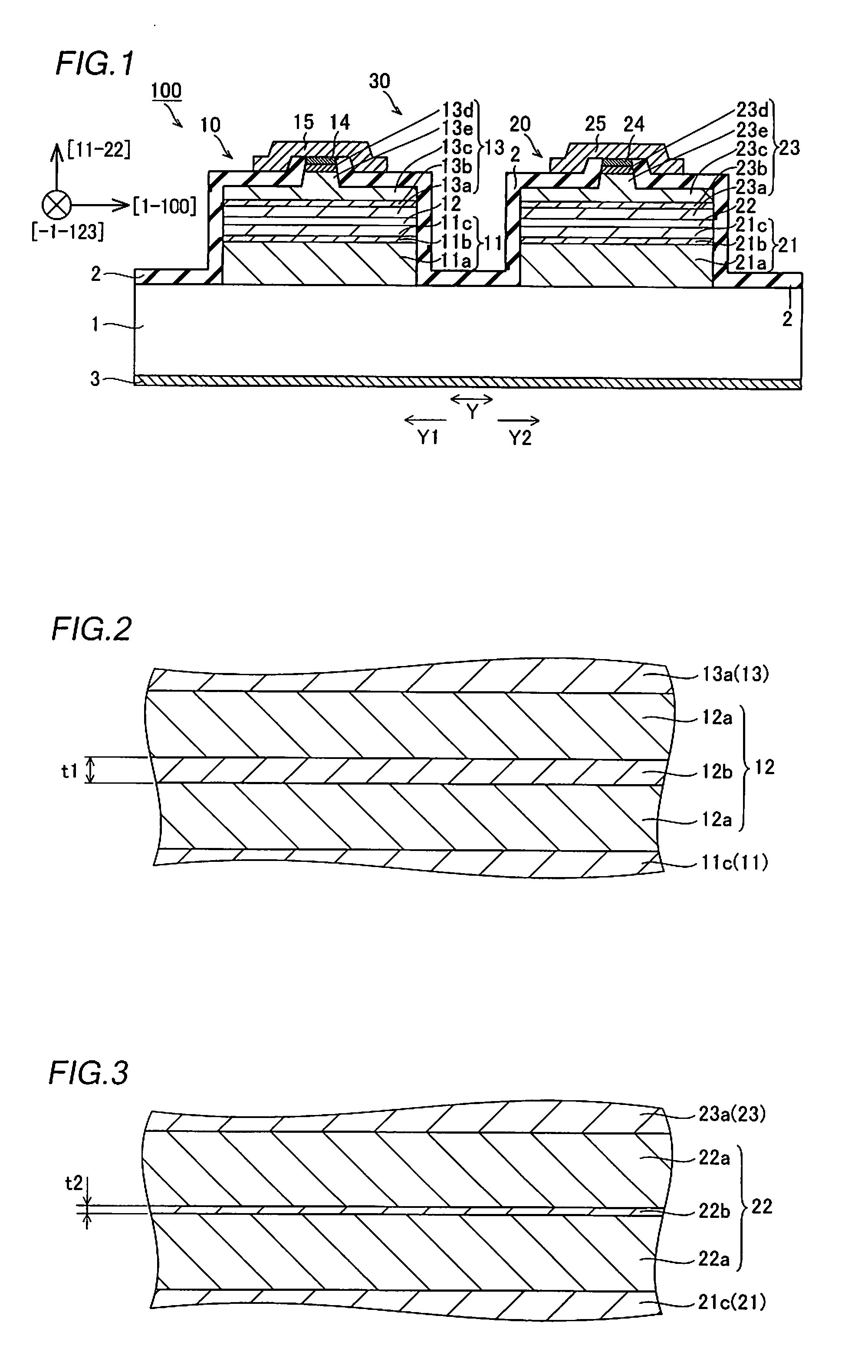
[0041]The structure of a semiconductor laser device 100 according to a first embodiment of the present invention is now described with reference to FIGS. 1 to 3.

[0042]In the semiconductor laser device 100 according to the first embodiment, a monolithic blue / green double-wavelength semiconductor laser element portion 30 consisting of a blue semiconductor laser element 10 having an oscillation wavelength of about 450 nm and a green semiconductor laser element 20 having an oscillation wavelength of about 530 nm is formed on an n-type GaN substrate 1 having a thickness of about 100 μm, as shown in FIG. 1. The blue semiconductor laser element 10 may be formed to have an oscillation wavelength in the range of about 435 nm to about 485 nm. The green semiconductor laser element 20 may be formed to have an oscillation wavelength in the range of about 500 nm to about 565 nm. The n-type GaN substrate 1 is an example of the “substrate” in the present invention.

[0043]The monolithic blue / green do...

second embodiment

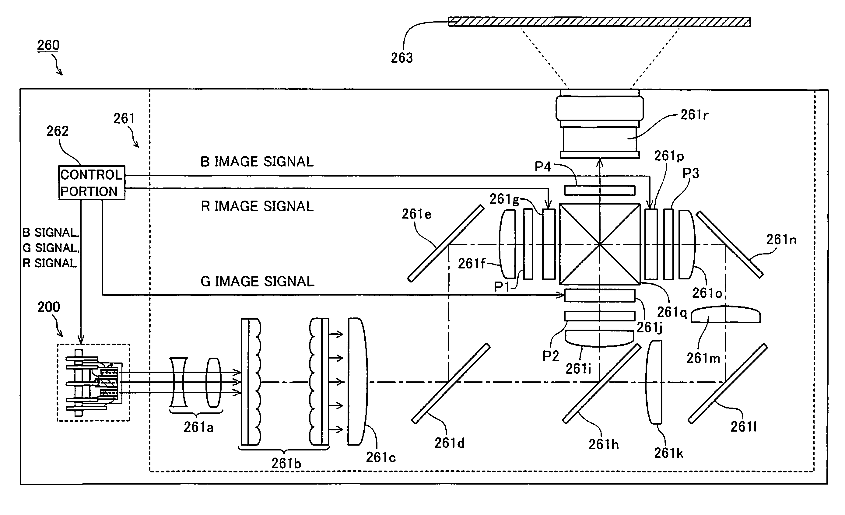
[0080]A semiconductor laser device 200 according to a second embodiment of the present invention is now described with reference to FIGS. 7 to 10. In the semiconductor laser device 200 according to the second embodiment, a red semiconductor laser element 240 is bonded onto an n-type GaN substrate 1 provided with a monolithic blue / green double-wavelength semiconductor laser element portion 30, dissimilarly to the aforementioned first embodiment. Projectors 250 and 260 each including the semiconductor laser device 200 are also described.

[0081]First, the structure of the semiconductor laser device 200 according to the second embodiment of the present invention is described with reference to FIG. 7.

[0082]In the semiconductor laser device 200 according to the second embodiment of the present invention, the red semiconductor laser element 240 having an oscillation wavelength of about 640 nm is bonded onto the upper surface of the n-type GaN substrate 1 on the side of a [1-100] direction (...


PUM


Abstract

This semiconductor laser device includes a substrate, a blue semiconductor laser element, formed on the surface of a substrate, including a first active layer made of a nitride-based semiconductor and having a first major surface of a non-C plane and a green semiconductor laser element, formed on the surface of the substrate, including a second active layer made of a nitride-based semiconductor and having a second major surface of a surface orientation substantially identical to the non-C plane.

Description

CROSS-REFERENCE TO RELATED APPLICATIONS [0001]The priority application numbers JP2008-251967, semiconductor laser device, Sep. 30, 2008, Yasumitsu Kunoh et al. and JP2009-198151, semiconductor laser device, Aug. 28, 2009, Yasumitsu Kunoh et al., upon which this patent application is based are hereby incorporated by reference.BACKGROUND OF THE INVENTION[0002]1. Field of the Invention[0003]The present invention relates to a semiconductor laser device and a display, and more particularly, it relates to a semiconductor laser device formed by integrating a plurality of semiconductor laser elements and a display including the same.[0004]2. Description of the Background Art[0005]While miniaturization of a device such as a projector has recently been increasingly required, development of a projector and a display each employing semiconductor laser elements as red (R), G (green) and B (blue) light sources is advanced. In order to miniaturize the device and to reduce the number of components ...

Claims


Application Information

Patent Timeline
IPC IPC(8): H01S5/40G09G3/20
CPCB82Y20/00G09G3/002G09G3/3406G09G3/346G09G2300/0452H04N9/3197H01S5/34333H01S5/4031H01S5/4087H04N9/3161G09G2310/0235
Inventor KUNOH, YASUMITSUNOMURA, YASUHIKO
Owner SANYO ELECTRIC CO LTD
Why Eureka
Try Eureka