
Liquid crystal device, electronic apparatus, and method of manufacturing liquid crystal device

Active Publication Date: 2010-04-01
JAPAN DISPLAY WEST
View PDF18 Cites 50 Cited by
  • Summary
  • Abstract
  • Description
  • Claims
  • Application Information

AI Technical Summary

Benefits of technology

[0012]An advantage of some aspects of the invention is that it provides a liquid crystal device having an excellent electrostatic protection function and capable of suppressing display quality reduction resulting from external static electricity and achieving a small thickness. Another advantage of some aspects of the invention is that it provides an electronic apparatus including such a liquid crystal device.

Problems solved by technology

For this reason, there is a problem in terms of display quality in that such a liquid crystal device is likely to be affected by electric fields (external electric fields) from outside of the counter substrate, typically static electricity, and thus, irregularities in the liquid crystal display are likely to occur.
As described above, in the case of arranging the electrostatic shielding layer on the outer surface, since the electrostatic shielding layer cannot be arranged prior to the polishing step, anti-static electricity measures are insufficient in the previous steps of the polishing step.
When the electrostatic shielding layer is arranged after the polishing step, namely after the pair of substrates is bonded together, the element substrate and the counter substrate are exposed to the high-temperature in a vacuum, the forming material (typically, resin) of the sealing member or a color filter layer may be deteriorated or peelings may occur at the interface or the inside of the resin.
For this reason, in the configuration of having the electrostatic shielding layer at the outer side of the glass substrate of the counter substrate, it is difficult to achieve the anti-static electricity measures (namely, the improvement in the display quality) and a small thickness of the liquid crystal device.
For this reason, a vertical electric field is generated between the electrostatic shielding layer for trapping static electricity and the pixel electrodes or the common electrodes provided on the element substrate, thus disadvantageously disturbing the lateral electric field mode driving.
Therefore, the anti-static electricity measures of the liquid crystal device are insufficient.
Since there is no underlying layer, it is practically impossible to form an alignment mark in advance and it is thus difficult to apply a mask film forming method that positions a mask on the counter substrate body 21 to form a film on a local area of the counter substrate body 21.
In the case of having such a shape, namely when the end faces are even with each other, static electricity can easily enter and the corrosion of the electrostatic shielding layer 40 is likely to occur.
According to such a configuration, since the electrostatic shielding layer and the liquid crystal layer are spaced apart by at least the thickness of the overcoat layer, thus causing a voltage drop, it is possible to weaken the force (coulomb force) of the static electricity trapped in the electrostatic shielding layer acting on the liquid crystal layer.

Method used


Image

  • Liquid crystal device, electronic apparatus, and method of manufacturing liquid crystal device
  • Liquid crystal device, electronic apparatus, and method of manufacturing liquid crystal device
  • Liquid crystal device, electronic apparatus, and method of manufacturing liquid crystal device

Examples


first embodiment

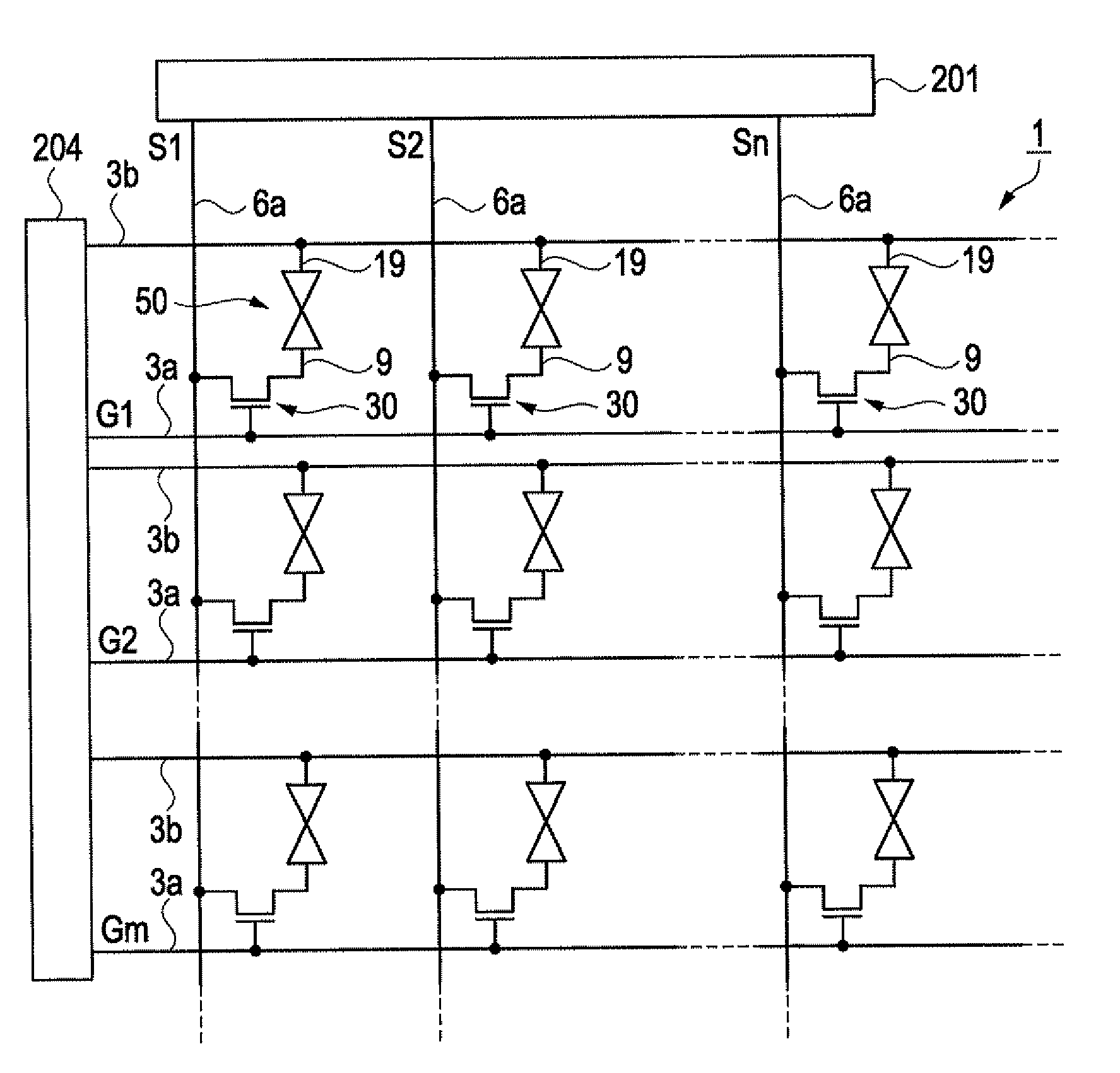
[0051]A liquid crystal device 1 according to a first embodiment of the invention will be described herein below with reference to FIGS. 1 to 5. In the drawings below, individual members are appropriately depicted with different thicknesses and measurements in order to make them recognizable in the drawings.

[0052]The liquid crystal device according to the present embodiment displays images by controlling the azimuth angle of liquid crystal molecules by using a lateral electric field perpendicular to the light traveling direction. An IPS (In-Plane Switching) mode and an FFS (Fringe-Field Switching) mode are known as examples of such a lateral electric field mode. Although the descriptions below are based on a liquid crystal device capable of performing full-color display in liquid crystal devices employing an FFS mode driving method, the invention can be equally applied to an IPS mode liquid crystal device.

[0053]FIG. 1 is an equivalent circuit diagram of a liquid crystal device 1 acco...

second embodiment

[0105]Next, a liquid crystal device 2 according to a second embodiment of the invention will be described. FIG. 7 is a simplified cross-sectional view of the liquid crystal device 2 according to the second embodiment of the invention, which corresponds to FIG. 6 in the first embodiment. Therefore, the configurations of the non-display area are not illustrated.

[0106]The liquid crystal device 2 according to the present embodiment has a similar configuration to the liquid crystal device 1 according to the first embodiment, except that the light shielding layer 22b , the coloring layer 22a , and the electrostatic shielding layer 40 are arranged differently on the counter substrate 20. In the descriptions of the present embodiment, drawings corresponding to FIGS. 1 to 4 are omitted. Moreover, the same constituent elements as those of the liquid crystal device 1 will be denoted by the same reference numerals, and the detailed descriptions thereof will be appropriately omitted.

[0107]As ill...

third embodiment

[0112]Next, a method of manufacturing the liquid crystal device according to a third embodiment of the invention will be described. FIGS. 9A to 9D are cross-sectional views illustrating the process steps of the liquid crystal device manufacturing method according to the third embodiment of the invention. The manufacturing method according to the present embodiment relates to the process steps for forming the electrostatic shielding layer. Therefore, only the constituent elements necessary for the present embodiment such as the counter substrate body 21 will be illustrated and other constituent elements will not be illustrated. The respective steps will be described below.

[0113]The manufacturing method according to the present embodiment will be illustrated with respect to the case of simultaneously forming a plurality of liquid crystal devices using a large-format (large-area) substrate.

[0114]First, as illustrated in FIG. 9A, a light shielding material layer 62 is formed on the enti...


PUM


Abstract

Provided is a lateral electric field mode liquid crystal device including: a first substrate; a second substrate; a liquid crystal layer and pixel electrodes and common electrodes. A lateral electric field mode liquid crystal device drives the liquid crystal layer by an electric field generated between the pixel electrodes and the common electrodes, a light shielding layer is formed on a surface of the second substrate disposed close to the liquid crystal layer. A coloring layer is also formed so as to overlap with the pixel electrodes. An overcoat layer protects the coloring layer, and an alignment film is formed. An electrostatic shielding layer is formed of a transparent conductive material on a surface of the overcoat layer.

Description

BACKGROUND[0001]1. Technical Field[0002]The present invention relates to a liquid crystal device, an electronic apparatus, and a method of manufacturing a liquid crystal device.[0003]2. Related Art[0004]As a means for achieving a wide viewing angle of a liquid crystal device, an IPS (In-Plane Switching) mode, which is one example of a so-called lateral electric field mode, has been put into practical use, in which an electric field is generated in an in-plane direction (lateral direction) to a substrate, the lateral electric field causes liquid crystal molecules contained in a liquid crystal layer to be rotated in a plane parallel of the substrate, thus controlling the transmission of light. Further, an FFS (Fringe-Field Switching) mode is proposed as an improvement of the IPS mode.[0005]Such a lateral electric field mode liquid crystal device has a configuration in which electrodes such as common electrodes and pixel electrodes or conductive members such as wirings are arranged on ...

Claims


Application Information

Patent Timeline
IPC IPC(8): G02F1/1333G02F1/13
CPCG02F2001/133334G02F1/134363G02F1/133334G02F1/1335
Inventor YOSHIDA, SHUHEITANAKA, SHINICHIRONISHIMURA, JOJIYOSHIDA, KOJITAKIZAWA, KEIJIHIGA, MASAKATSU
Owner JAPAN DISPLAY WEST
Features
  • Generate Ideas
  • Intellectual Property
  • Life Sciences
  • Materials
  • Tech Scout
  • Unparalleled Data Quality
  • Higher Quality Content
  • 60% Fewer Hallucinations
Learn More