Method of forming a diffusion barrier and adhesion layer for an interconnect structure

Inactive Publication Date: 2010-04-01
TOKYO ELECTRON LTD
View PDF8 Cites 24 Cited by
  • Summary
  • Abstract
  • Description
  • Claims
  • Application Information

AI Technical Summary

Benefits of technology

[0007]A method of forming an interconnect structure for an integrated circuit is provided. The interconnect structure contains an interconnect opening within a dielectric material having a diffusion barrier formed from a la

Problems solved by technology

As the width of metal lines is scaled down to smaller submicron and even nanometer dimensions, electromigration failure, which may lead to open and extruded metal lines, is now a well-recogniz

Method used


Image

  • Method of forming a diffusion barrier and adhesion layer for an interconnect structure
  • Method of forming a diffusion barrier and adhesion layer for an interconnect structure
  • Method of forming a diffusion barrier and adhesion layer for an interconnect structure

Examples


Example

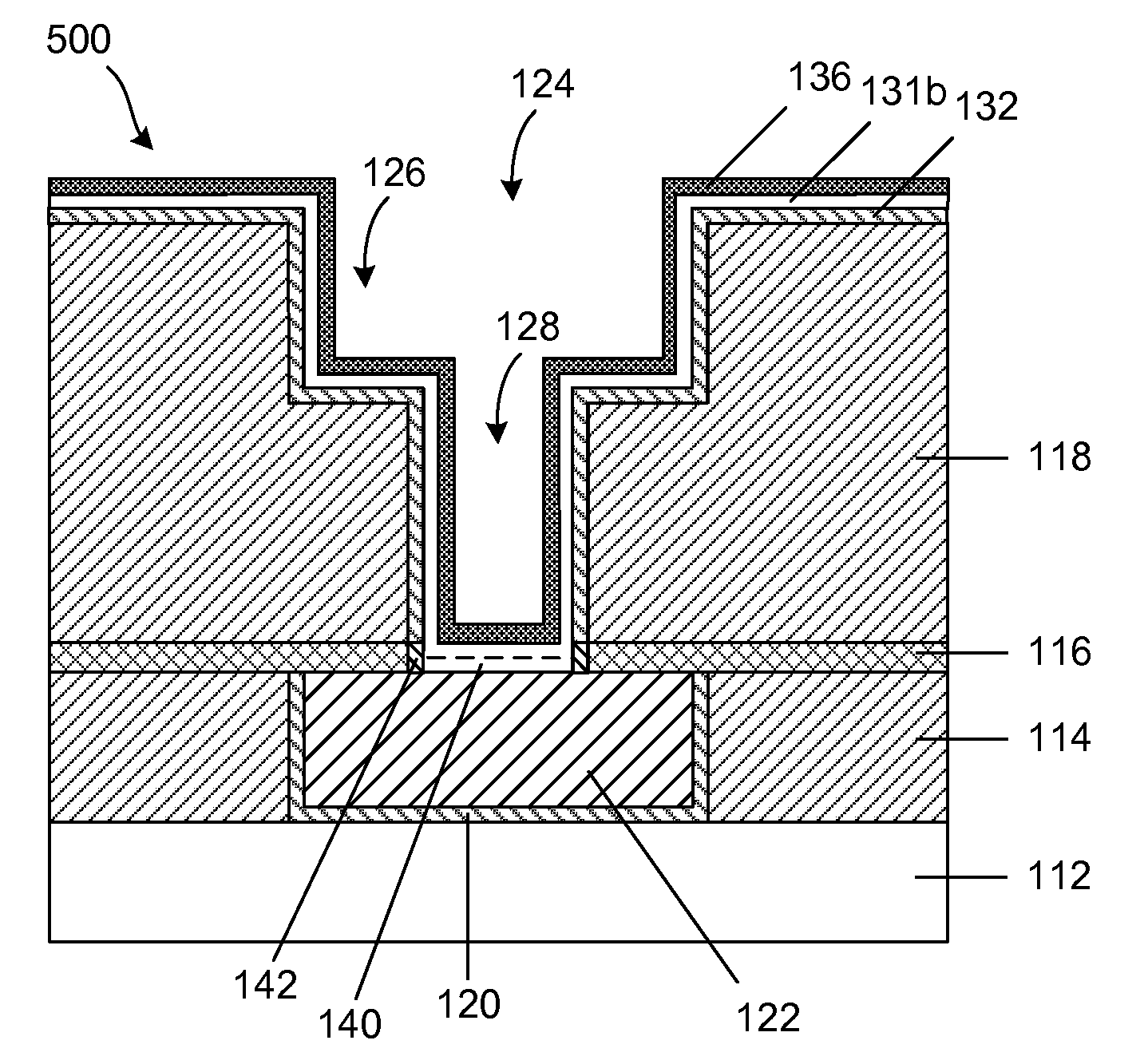
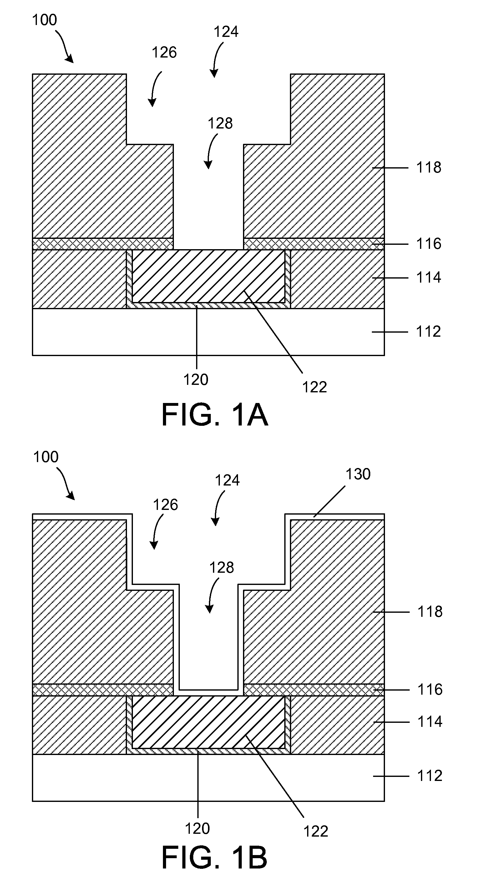
[0017]Embodiments of the invention provide interconnect structures for integrated circuits and method of forming the interconnect structures. The interconnect structures include a cobalt compound diffusion barrier that prevents diffusion of Cu metal into a dielectric material in an interconnect opening and further contains a cobalt nitride adhesion layer on the diffusion barrier that provides good adhesion to the Cu metal and an optional Ru seed layer on the cobalt nitride adhesion layer.

[0018]Referring now to the drawings,FIGS. 1A-1L schematically show cross-sectional views for forming interconnect structures containing dual damascene openings according to embodiments of the invention. FIG. 1A schematically shows a cross-sectional view of an interconnect structure 100 containing a dual damascene interconnect opening 124 formed over a conductive interconnect structure 122. Dual damascene interconnect openings are well known to one of ordinary skill in the art of integrated circuit f...


PUM


Abstract

A method of forming an interconnect structure is provided. The method includes depositing a cobalt metal layer in an interconnect opening formed within a dielectric material containing a dielectric reactant element. The method further includes, in any order, thermally reacting at least a portion of the cobalt metal layer with at least a portion of the dielectric material to form a diffusion barrier containing a compound of the reactive metal from the cobalt metal layer and the dielectric reactant element from the dielectric material, and forming a cobalt nitride adhesion layer in the interconnect opening. The method further includes filling the interconnect opening with Cu metal, where the diffusion barrier and the cobalt nitride adhesion layer surround the Cu metal in the interconnect opening.

Description

CROSS-REFERENCE TO RELATED APPLICATIONS[0001]This application is related to co-pending U.S. patent application Ser. No. 11 / 691,167 entitled “DIFFUSION BARRIER FOR INTEGRATED CIRCUITS FORMED FROM A LAYER OF A REACTIVE METAL AND METHOD OF FABRICATION”, filed on Mar. 26, 2007. This application is related to co-pending U.S. patent application Ser. No. ______ (Docket no. TTCA-291) entitled “DIFFUSION BARRIER AND ADHESION LAYER FOR AN INTERCONNECT STRUCTURE”, filed on even date herewith. The entire contents of these applications are herein incorporated by reference in their entirety.FIELD OF THE INVENTION[0002]The invention relates generally to fabrication of interconnect structures within integrated circuits, and more particularly, to using a layer of cobalt metal for forming a diffusion barrier on dielectric materials within the interconnect structure and a cobalt nitride adhesion layer on the diffusion barrier.BACKGROUND OF THE INVENTION[0003]An integrated circuit contains various semi...

Claims


Application Information

Patent Timeline
IPC IPC(8): H01L21/4763
CPCH01L21/76831H01L21/76844H01L21/76846H01L21/76873H01L21/76856H01L21/76858H01L21/76855H01L23/53238
Inventor ISHIZAKA, TADAHIROMIZUNO, SHIGERU
Owner TOKYO ELECTRON LTD
Why Eureka
Try Eureka