Impedance optimized interface for membrane probe application

a membrane probe and interface technology, applied in the field of probe assemblies, can solve the problems of excessive force erratic performance of the probe system, and damage to the bond pad,

Active Publication Date: 2010-04-08
FORMFACTOR INC
View PDF102 Cites 12 Cited by
  • Summary
  • Abstract
  • Description
  • Claims
  • Application Information

AI Technical Summary

Problems solved by technology

However, inconsistencies in connections with the ground plane of the interface board may cause the impedance of a particular signal path to vary from the desired matched impedance producing a reflection of the RF signals that are absorbed by other structures resulting in erratic performance of the probing system.
While penetration of the oxide layer improves conductivity, excessive force can damage the bond pad.
However, the conductors within the membrane assembly and attached to the

Method used


Image

  • Impedance optimized interface for membrane probe application
  • Impedance optimized interface for membrane probe application
  • Impedance optimized interface for membrane probe application

Examples


Embodiment Construction

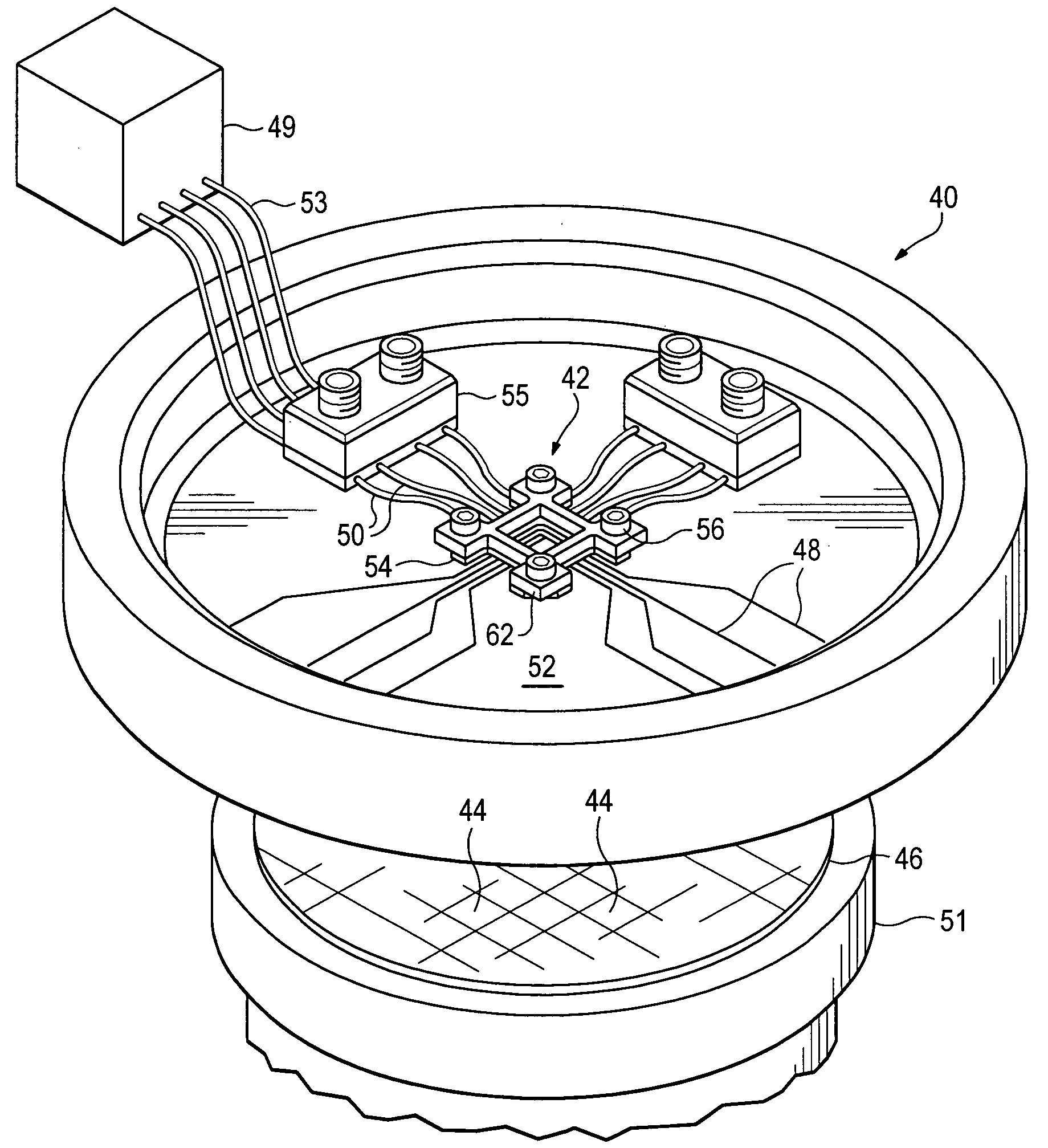
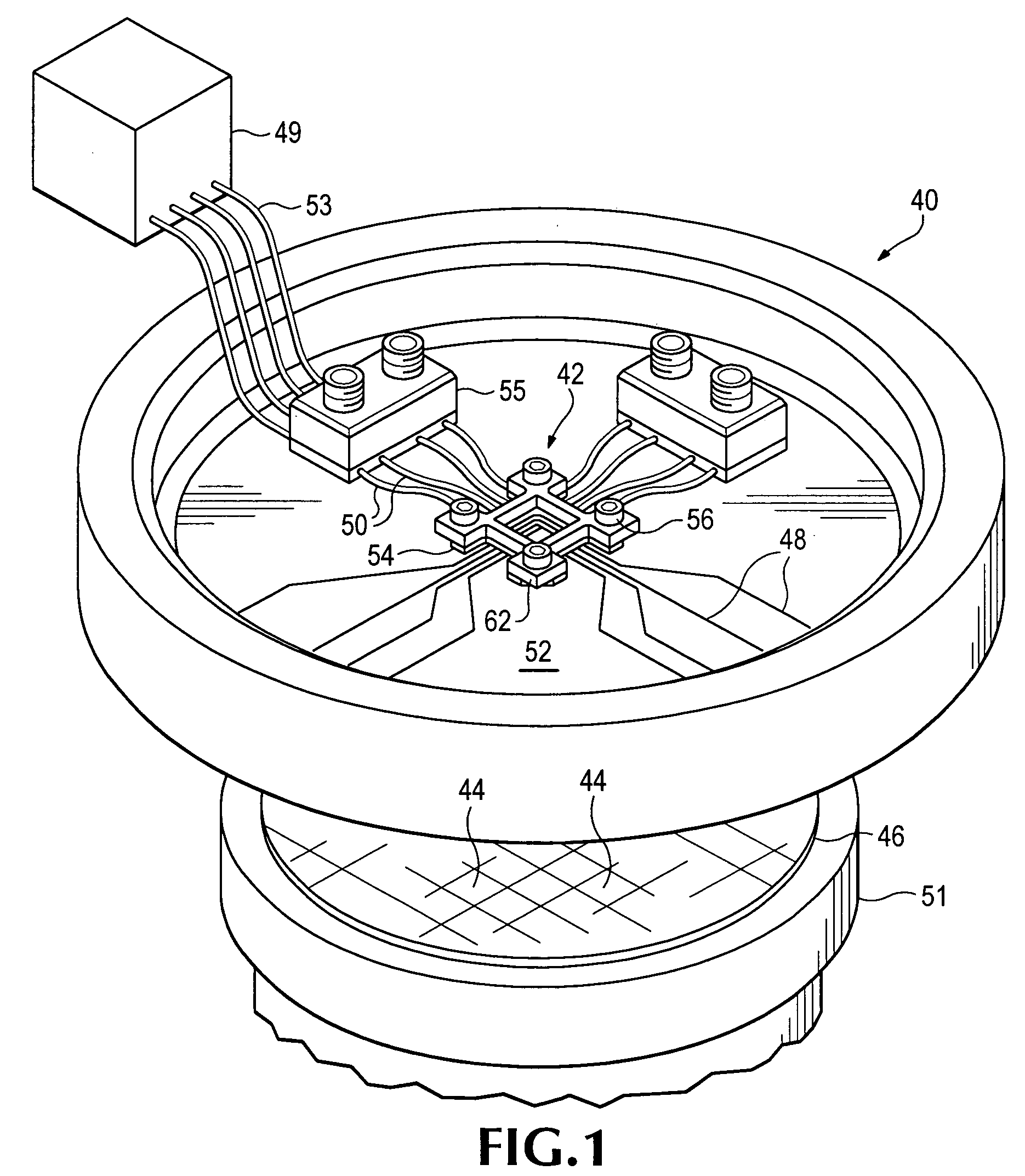
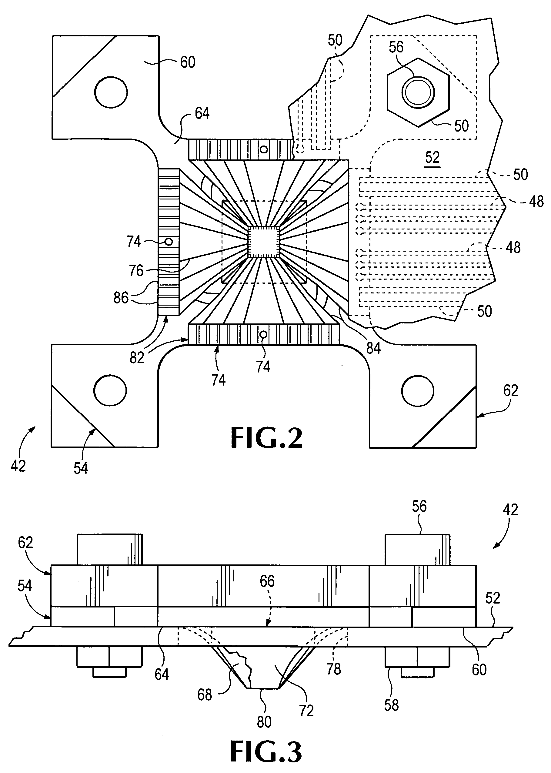
[0030]Referring in detail to the drawings where similar parts are identified by like reference numerals, and, more particularly to FIGS. 1 and 4, a probe head 40 for mounting a membrane probing assembly 42 is illustrated. In order to measure the electrical performance of the electrical circuit or device-under-test (DUT) of a particular die area 44 included on the silicon wafer 46, input and output ports of the test instrumentation 49 are communicatively connected to contacts 81 included on the lower portion of the membrane probing assembly and the chuck 51 which supports the wafer is moved in mutually perpendicular X, Y, and Z directions in order to bring bond pads of the DUT into pressing engagement with the probe's contacts.

[0031]The probe head 40 includes an interface board 52 on which traces 48 and shielded transmission lines are arranged for communicating data, signals and power between the test instrumentation and the DUT. Typically, high frequency signals are communicated bet...


PUM


Abstract

In a membrane probing apparatus, the impedance of the interface between coaxial cables connected to the test instrumentation and the membrane supported co-planar waveguide that conductively connects to the probe's contacts is optimized by eliminating a ground plane in the interface board.

Description

CROSS-REFERENCE TO RELATED APPLICATIONS[0001]Not applicable.BACKGROUND OF THE INVENTION[0002]The present invention relates to probe assemblies of the type commonly used for testing integrated circuits (ICs) that are fabricated on a wafer or substrate.[0003]The trend in electronic production, particularly in integrated circuit technology, has been toward fabricating larger numbers of discrete circuit elements with higher operating frequencies and smaller geometries on a single substrate or “wafer.” After fabrication, the wafer is divided into a number of rectangular-shaped chips or “dies” where each die presents a rectangular or other regular arrangement of metallic bond or contact pads through which connections are made for the inputs and outputs of the electrical circuit on the die. Although each die is eventually packaged separately, for efficiency sake, testing of the circuits formed on the wafer is preferably performed while the dies are still joined together on the wafer. One t...

Claims


Application Information

Patent Timeline
IPC IPC(8): G01R31/00
CPCG01R1/07378G01R1/06772
Inventor SMITH, KENNETH R.HAYWARD, ROGER
Owner FORMFACTOR INC
Why Eureka
Try Eureka