Chip package structure with shielding cover

a shielding cover and chip technology, applied in the direction of semiconductor devices, semiconductor/solid-state device details, small component housings, etc., can solve the problems of shift and deflection of the metal cover, the inability of the cover disposed on the circuit board to be accurately positioned, and the electronic signals are easier to suffer electromagnetic interference, so as to improve the yield of assembly

Active Publication Date: 2010-04-08
ADVANCED SEMICON ENG INC
View PDF21 Cites 23 Cited by
  • Summary
  • Abstract
  • Description
  • Claims
  • Application Information

AI Technical Summary

Benefits of technology

[0007]The present invention is directed to a chip package structure with a shielding cover for improving yield of assembling the shielding cover.

Problems solved by technology

Nevertheless, the higher a clock frequency of the IC chip is, the easier the electronic signals suffer from electromagnetic interference (EMI).
Nonetheless, in a process of baking and solidifying the conductive paste or in a reflow process for transforming the solder paste to be in a liquid form, heat convection generated thereby results in shift and deflection of the metal cover.
As a result, the metal cover disposed on the circuit board cannot be accurately positioned on the pads of the circuit board, and yield of assembling the metal cover is negatively affected.

Method used


Image

  • Chip package structure with shielding cover
  • Chip package structure with shielding cover
  • Chip package structure with shielding cover

Examples


Embodiment Construction

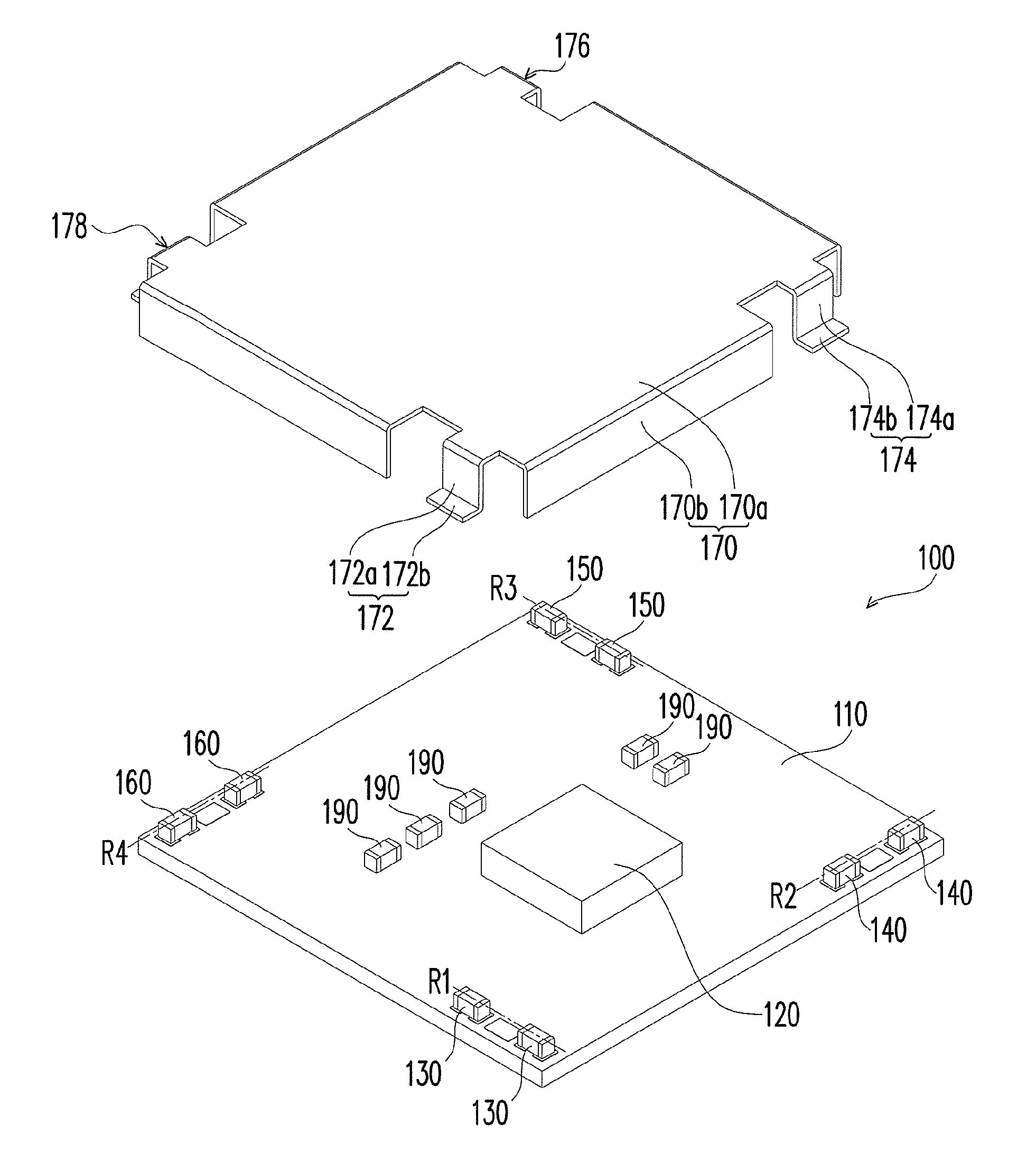
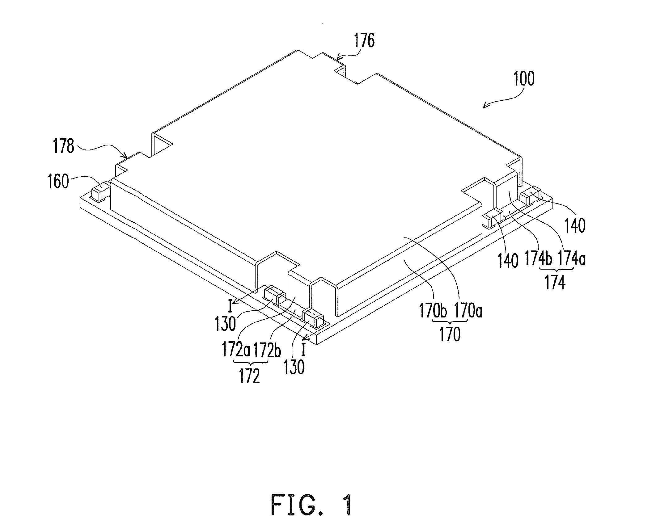
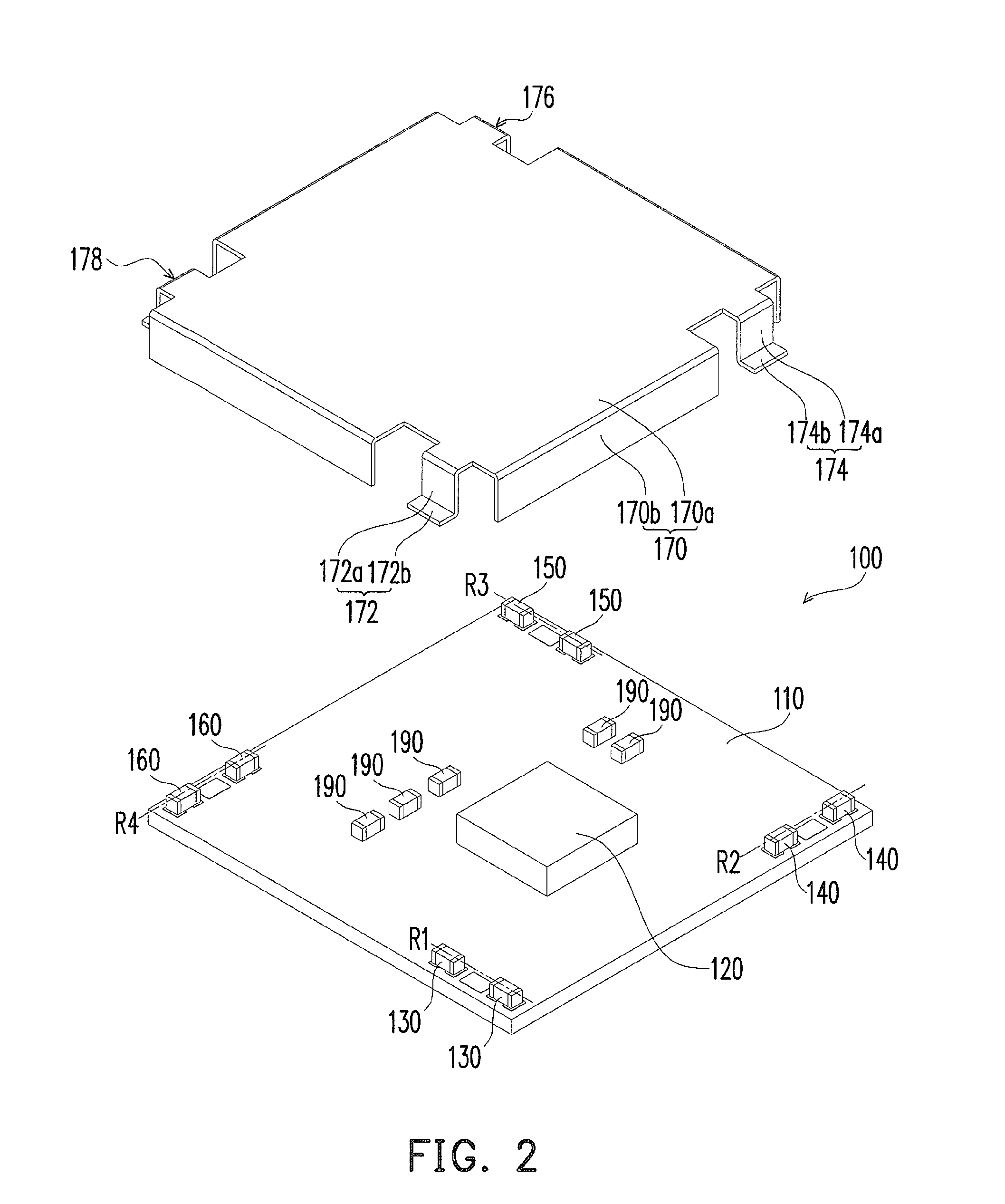
[0025]FIG. 1 is a schematic three-dimensional view of a chip package structure with a shielding cover according to an embodiment of the present invention. FIG. 2 is a schematic three-dimensional exploded view of the chip package structure with the shielding cover as depicted in FIG. 1. FIG. 3 is a cross-sectional view which is taken along a line I-I and illustrates the chip package structure with the shielding cover as depicted in FIG. 1. Referring to FIGS. 1 and 2, in the present embodiment, a chip package structure 100 includes a substrate 110, a chip 120, a pair of first passive components 130, a pair of second passive components 140, and a shielding cover 170. According to the present embodiment, the substrate 110 is, for example, a printed circuit board (PCB), a module board, or a package substrate.

[0026]Specifically, the chip 120 is disposed on the substrate 110. Besides, the chip 120 can be electrically connected to the substrate 110 through a plurality of conductive bumps (n...


PUM


Abstract

A chip package structure with a shielding cover includes a substrate, a chip, a pair of first passive components, a pair of second passive components, and a shielding cover. The chip, the pair of first passive components, the pair of second passive components, and the shielding cover are disposed on the substrate. The chip is electrically connected to the substrate. The shielding cover covers the chip and has leads connected to the substrate. The leads include a first lead and a second lead. The first lead connected to a portion of the substrate is located between the pair of first passive components and arranged along a first axis with the pair of first passive components. The second lead connected to a portion of the substrate is located between the pair of second passive components and arranged along a second axis with the pair of second passive components.

Description

CROSS-REFERENCE TO RELATED APPLICATION[0001]This application claims the priority benefit of Taiwan application serial no. 97138564, filed Oct. 7, 2008. The entirety of the above-mentioned patent application is hereby incorporated by reference herein and made a part of specification.BACKGROUND OF THE INVENTION[0002]1. Field of the Invention[0003]The present invention relates to a chip package structure, and more particularly to a chip package structure with a shielding cover.[0004]2. Description of Related Art[0005]An integrated circuit (IC) chip is often electrically connected to a motherboard through a circuit board, so as to allow electronic signals to be transmitted between the IC chip and the motherboard. Nevertheless, the higher a clock frequency of the IC chip is, the easier the electronic signals suffer from electromagnetic interference (EMI). In order to prevent stability of the IC chip from being affected by EMI, a metal cover is frequently disposed on top of the circuit bo...

Claims


Application Information

Patent Timeline
Patent Type & Authority Applications(United States)
IPC IPC(8): H05K9/00
CPCH05K5/0091H05K9/0026H01L2924/19105H01L2224/16225H01L23/552
Inventor LU, HSIN-CHIEHCHOU, CHIN-FENG
Owner ADVANCED SEMICON ENG INC
Why Eureka
Try Eureka