Silicon-based nanoscale resistive device with adjustable resistance

a nano-scale, resistive device technology, applied in semiconductor devices, digital storage, instruments, etc., can solve the problems of limiting production yields and reducing the resistance of a-si structures

Active Publication Date: 2010-04-08
RGT UNIV OF MICHIGAN
View PDF13 Cites 283 Cited by
  • Summary
  • Abstract
  • Description
  • Claims
  • Application Information

AI Technical Summary

Benefits of technology

[0006]In accordance with one aspect of the invention, there is provided a non-volatile solid state resistive device, comprising a first electrode, a p-type silicon second electrode, and a non-crystalline silicon nanostructure electrically connected between the electrodes. T

Problems solved by technology

In the case of a-Si structures, voltage-induced diffusion of metal ions into the silicon leads to the formation of conductive filaments that reduce the resistance of the a-Si structure.
However, such devices typically h

Method used


Image

  • Silicon-based nanoscale resistive device with adjustable resistance
  • Silicon-based nanoscale resistive device with adjustable resistance
  • Silicon-based nanoscale resistive device with adjustable resistance

Examples


Embodiment Construction

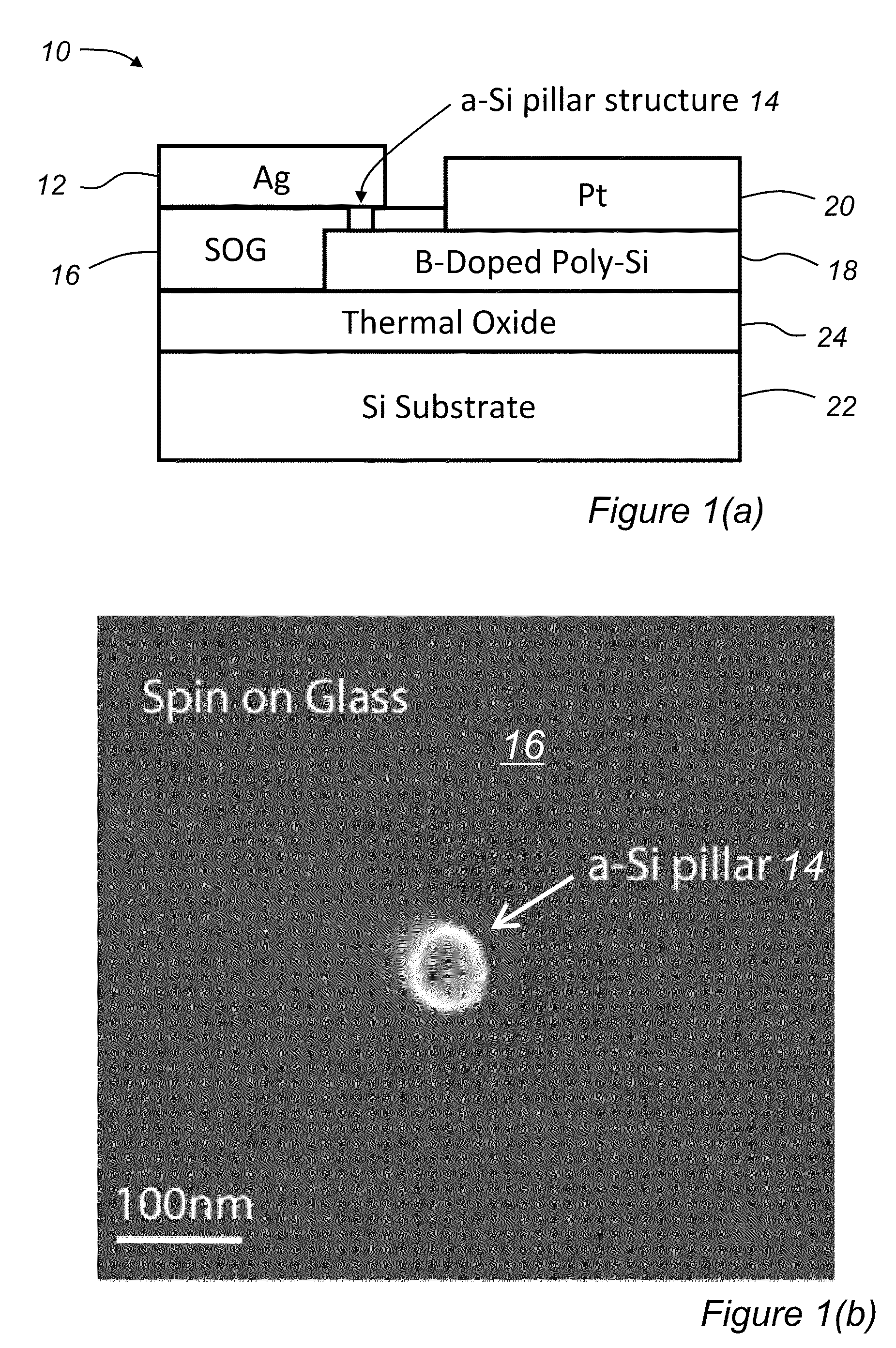
[0032]FIG. 1(a) depicts a non-volatile solid state resistive device 10 comprising a nanoscale a-Si structure 14 that exhibits a resistance that can be selectively set to various values, and reset, all using appropriate control circuitry. Once set, the resistance value can be read using a small voltage that is sufficient in magnitude to determine the resistance without causing it to change. Although the illustrated embodiment uses a-Si as the resistive element, it will be appreciated that other non-crystalline silicon (nc-Si) structures can be used, such as amorphous poly-silicon. Thus, as used herein and in the claims, non-crystalline silicon (nc-Si) means either amorphous silicon (a-Si), amorphous poly-silicon (poly-Si) that exhibits controllable resistance, or a combination of the two. Furthermore, although much of the discussion herein applies also to larger scale a-Si structures such as those having one or more dimensions in the micron range, the illustrated embodiment is an a-S...


PUM


Abstract

A non-volatile solid state resistive device that includes a first electrode, a p-type poly-silicon second electrode, and a non-crystalline silicon nanostructure electrically connected between the electrodes. The nanostructure has a resistance that is adjustable in response to a voltage being applied to the nanostructure via the electrodes. The nanostructure can be formed as a nanopillar embedded in an insulating layer located between the electrodes. The first electrode can be a silver or other electrically conductive metal electrode. A third (metal) electrode can be connected to the p-type poly-silicon second electrode at a location adjacent the nanostructure to permit connection of the two metal electrodes to other circuitry. The resistive device can be used as a unit memory cell of a digital non-volatile memory device to store one or more bits of digital data by varying its resistance between two or more values.

Description

CROSS-REFERENCE TO RELATED APPLICATION[0001]This application claims the benefit of Provisional Application No. 61 / 103,928 filed Oct. 8, 2008, the contents of which are hereby incorporated by reference.TECHNICAL FIELD[0002]The invention relates to two-terminal non-volatile solid state resistive devices having an adjustable resistance that can be used for memory storage and controllable circuit interconnects.BACKGROUND OF THE INVENTION[0003]Resistive random-access memories (RRAMs) have generated significant interest recently as a potential candidate for ultra-high density non-volatile information storage. A typical RRAM device consists of an insulator layer sandwiched between a pair of electrodes and exhibits electrical pulse induced hysteretic resistance switching effects. The resistance switching has been explained by the formation of conductive filaments inside the insulator due to Joule heating and electrochemical processes in binary oxides (e.g. NiO and TiO2) or redox processes f...

Claims


Application Information

Patent Timeline
IPC IPC(8): G11C11/00H01L47/00
CPCG11C11/56H01L45/148G11C13/003G11C13/0069G11C2213/11G11C2213/15G11C2213/33G11C2213/72G11C2213/76H01L27/2409H01L27/2436H01L27/2463H01L45/085H01L45/1233H01L45/1253G11C13/0002H10B63/20H10B63/30H10B63/80H10N70/245H10N70/841H10N70/884H10N70/826H10N70/20
Inventor LU, WEIJO, SUNG HYUNKIM, KUK-HWAN
Owner RGT UNIV OF MICHIGAN
Why Eureka
Try Eureka