

Method for reducing sidewall etch residue
- Summary
- Abstract
- Description
- Claims
- Application Information
AI Technical Summary
Benefits of technology
Problems solved by technology
Method used
Image

Examples
Embodiment Construction
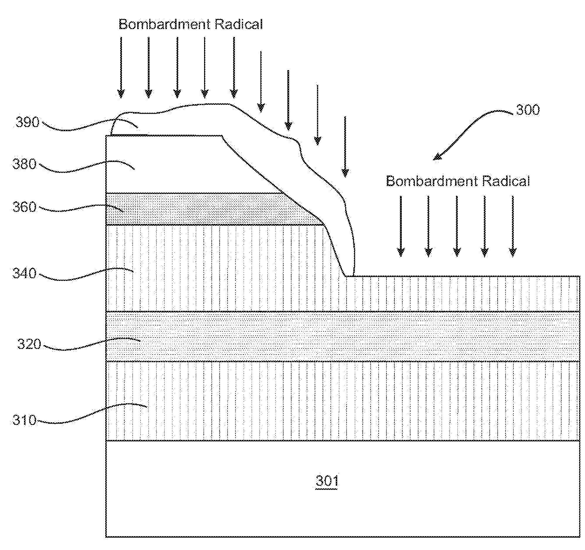
[0018]One or more aspects of the present invention will now be described with reference to the attached figures, wherein like reference numerals are used to refer to like elements throughout, and wherein the various structures are not necessarily drawn to scale.
[0019]The present invention relates to the methods of fabricating semiconductor devices in a manner that reduces the amount of etch residue remaining post etch. In general terms, a first layer is formed over a substrate followed by a second overlying layer. The second layer is isotropically etched to form a patterned second layer with outwardly tapered sidewalls and the first layer is subsequently etched in accordance with the second layer. During the etching of the first layer, etch residues are formed along the sidewalls of the first and second layer. The outwardly tapered sidewalls of the second layer may be inclined at an angle such that etch residues formed thereon can be dislodged more efficiently by physical bombardmen...
PUM
 Abstract
Description
Claims
Application Information