Nonvolatile Memory and Method With Reduced Program Verify by Ignoring Fastest and/or Slowest Programming Bits

Active Publication Date: 2010-04-15
SANDISK TECH LLC
View PDF23 Cites 47 Cited by
  • Summary
  • Abstract
  • Description
  • Claims
  • Application Information

AI Technical Summary

Benefits of technology

[0019]Since the programming pass is spanned by the series of pulses, a given pulse represents a given phase in the programming pass. A reference pulse is established and different verify levels are scheduled to be included in the verifying starting at different pulses relative to the reference pulse. The reference pulse is determined when a predetermined number of cells (the fastest cells) have first been program-verified relative to a first verify level. A subsequent verify level will start a certain number of pulses after the reference pulse based on an estimate of how many pulses to program from the first verify level to the subsequent verify level. Since the reference pulse is established after the predetermined number cells have been programm

Problems solved by technology

This amounts to skipping the verify and inhibit steps of the

Method used


Image

  • Nonvolatile Memory and Method With Reduced Program Verify by Ignoring Fastest and/or Slowest Programming Bits
  • Nonvolatile Memory and Method With Reduced Program Verify by Ignoring Fastest and/or Slowest Programming Bits
  • Nonvolatile Memory and Method With Reduced Program Verify by Ignoring Fastest and/or Slowest Programming Bits

Examples


Embodiment Construction

Memory System

[0053]FIG. 1 to FIG. 10 illustrate example memory systems in which the various aspects of the present invention may be implemented.

[0054]FIG. 11 and FIG. 12 illustrate a conventional programming technique.

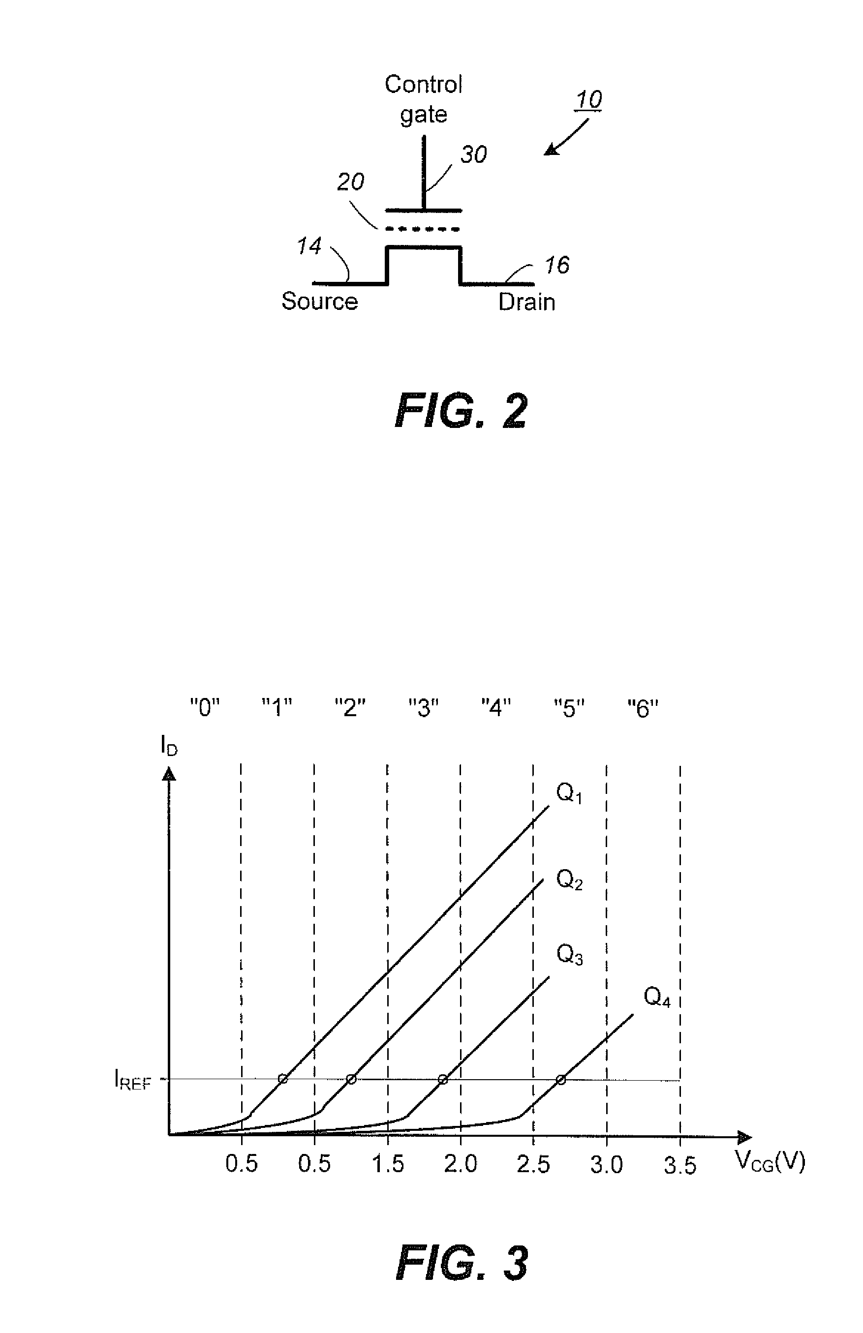
[0055]FIG. 13 to FIG. 22 illustrate the context and details of the various aspects and embodiments of the present invention.

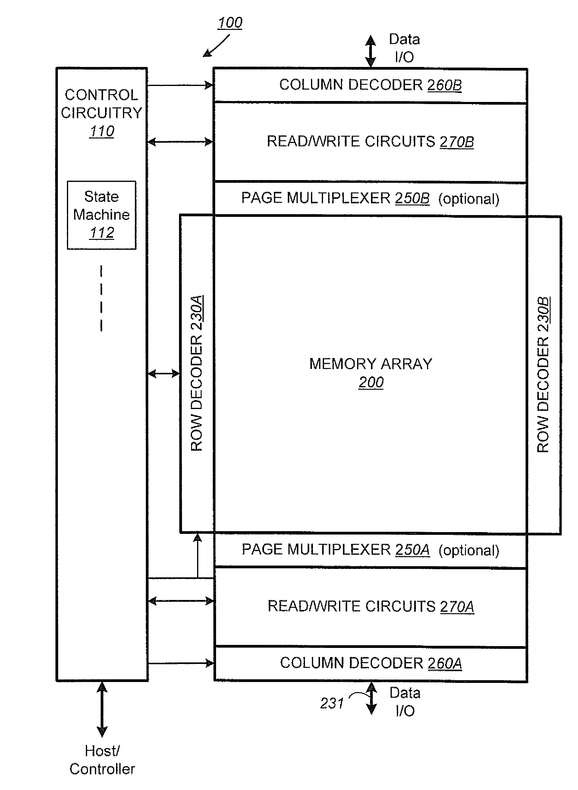
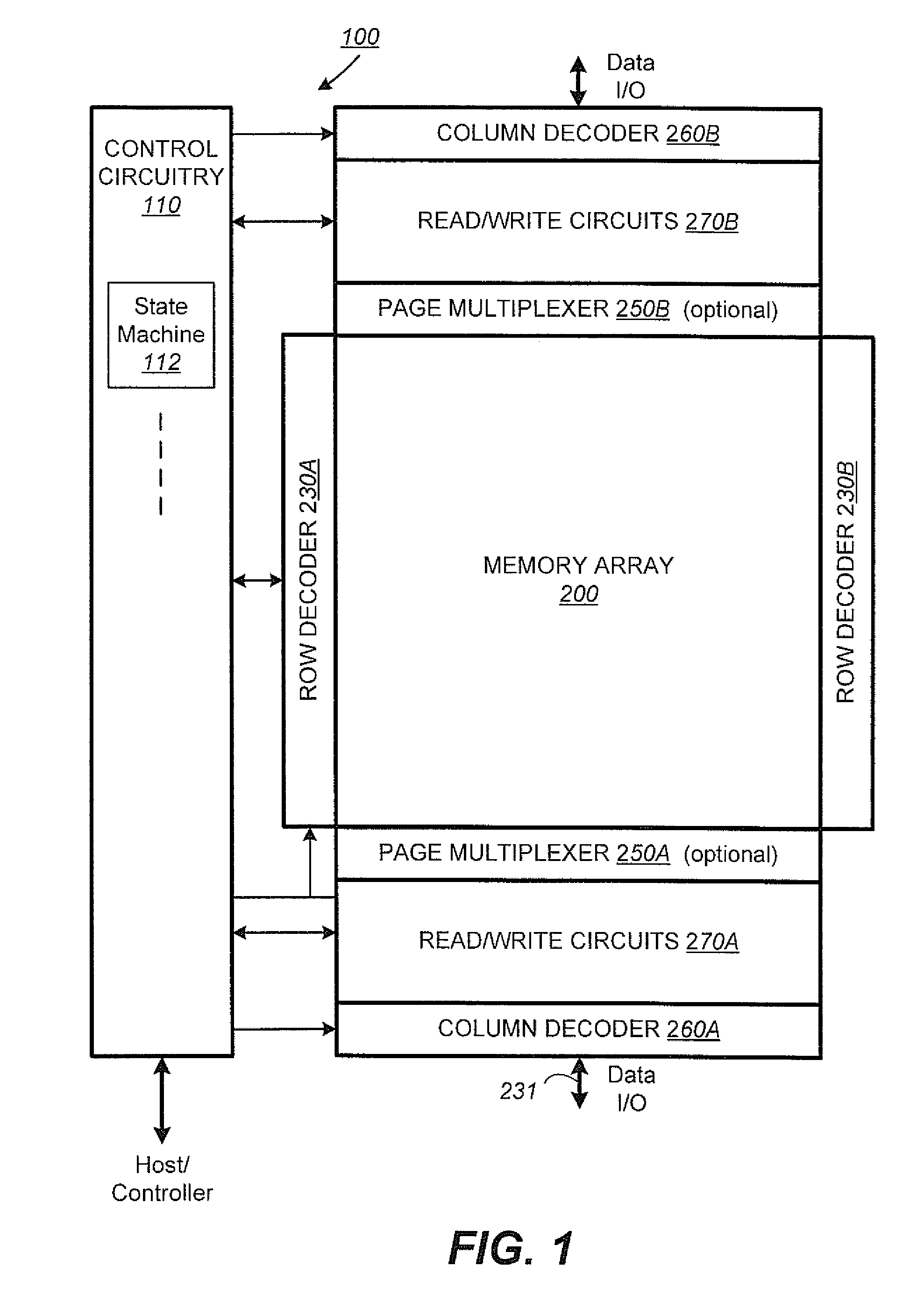
[0056]FIG. 1 illustrates schematically the functional blocks of a non-volatile memory chip in which the present invention may be implemented. The memory chip 100 includes a two-dimensional array of memory cells 200, control circuitry 210, and peripheral circuits such as decoders, read / write circuits and multiplexers.

[0057]The memory array 200 is addressable by word lines via row decoders 230 (split into 230A, 230B) and by bit lines via column decoders 260 (split into 260A, 260B) (see also FIGS. 4 and 5.) The read / write circuits 270 (split into 270A, 270B) allow a page of memory cells to be read or programmed in parallel. A data I / O bus 231 is coup...


PUM


Abstract

A group of non-volatile memory cells are programmed in a programming pass by a series of incremental programming pulses where each pulse is followed by a program-verify and possibly program-inhibition step. Performance is improved during the programming pass by delayed starting and prematurely terminating the various verify levels that demarcate the multiple memory states. This amounts to skipping the verifying and inhibiting steps of the fastest and slowest programming (fringe) cells of the group. A reference pulse is established when the fastest cells have all been program-verified relative to a first verify level. The starting of what verify level at what pulse will then be delayed relative to the reference pulse. Verifying stops for a given verify level when only a predetermined number of cells remain unverified relative to that given level. Any errors arising from over- or under-programming of the fringe cells are corrected by an error correction code.

Description

CROSS REFERENCE TO RELATED APPLICATIONS[0001]This application is a continuation of application Ser. No. 12 / 249,678, filed on Oct. 10, 2008, which application is incorporated herein in its entirety by this reference.FIELD OF THE INVENTION[0002]This invention relates generally to non-volatile semiconductor memory such as electrically erasable programmable read-only memory (EEPROM) and flash EEPROM, and specifically to memory and programming operations in which the number of verify operations are reduced by ignoring verifying of very fast and very slow programming cells.BACKGROUND OF THE INVENTION[0003]Solid-state memory capable of nonvolatile storage of charge, particularly in the form of EEPROM and flash EEPROM packaged as a small form factor card, has recently become the storage of choice in a variety of mobile and handheld devices, notably information appliances and consumer electronics products. Unlike RAM (random access memory) that is also solid-state memory, flash memory is non...

Claims


Application Information

Patent Timeline
IPC IPC(8): G11C16/04G11C16/06
CPCG11C11/5628G11C2211/5621G11C16/0483
Inventor LI, YANFONG, YUPIN KAWINGCHAN, SIU LUNG
Owner SANDISK TECH LLC
Why Eureka
Try Eureka