Bonding apparatus and bonding method

a technology of bonding apparatus and electrode, which is applied in the direction of soldering apparatus, auxillary welding device, semiconductor/solid-state device details, etc., can solve the problems of reducing production efficiency, reducing reliability of bonding, and requiring the carrying of a large number of semiconductor dies, so as to achieve efficient bonding of each electrode, simple and easy way, and strengthen bonding

Inactive Publication Date: 2010-04-15
SHINKAWA CO LTD
View PDF13 Cites 57 Cited by
  • Summary
  • Abstract
  • Description
  • Claims
  • Application Information

AI Technical Summary

Benefits of technology

[0028]It is preferable that the bonding method according to the present invention includes an underfill material application step of applying underfill material on to a surface to be bonded of one of the semiconductor die and the substrate to strengthen the bonding by provided in a gap either between the semiconductor die and the substrate or between semiconductor dies that are bonded to each ...

Problems solved by technology

H09-326416, a previously bonded portion can often be fused due to heat applied when bonding, reducing reliability in bonding.
However, when bonding a circuit board of a semiconductor die, the bonding of a large number of semiconductor dies is required to be carried out in a short period of time.
Therefore maintaining such conditions for such a long period of time in the middle of a bonding ...

Method used


Image

  • Bonding apparatus and bonding method
  • Bonding apparatus and bonding method
  • Bonding apparatus and bonding method

Examples


Embodiment Construction

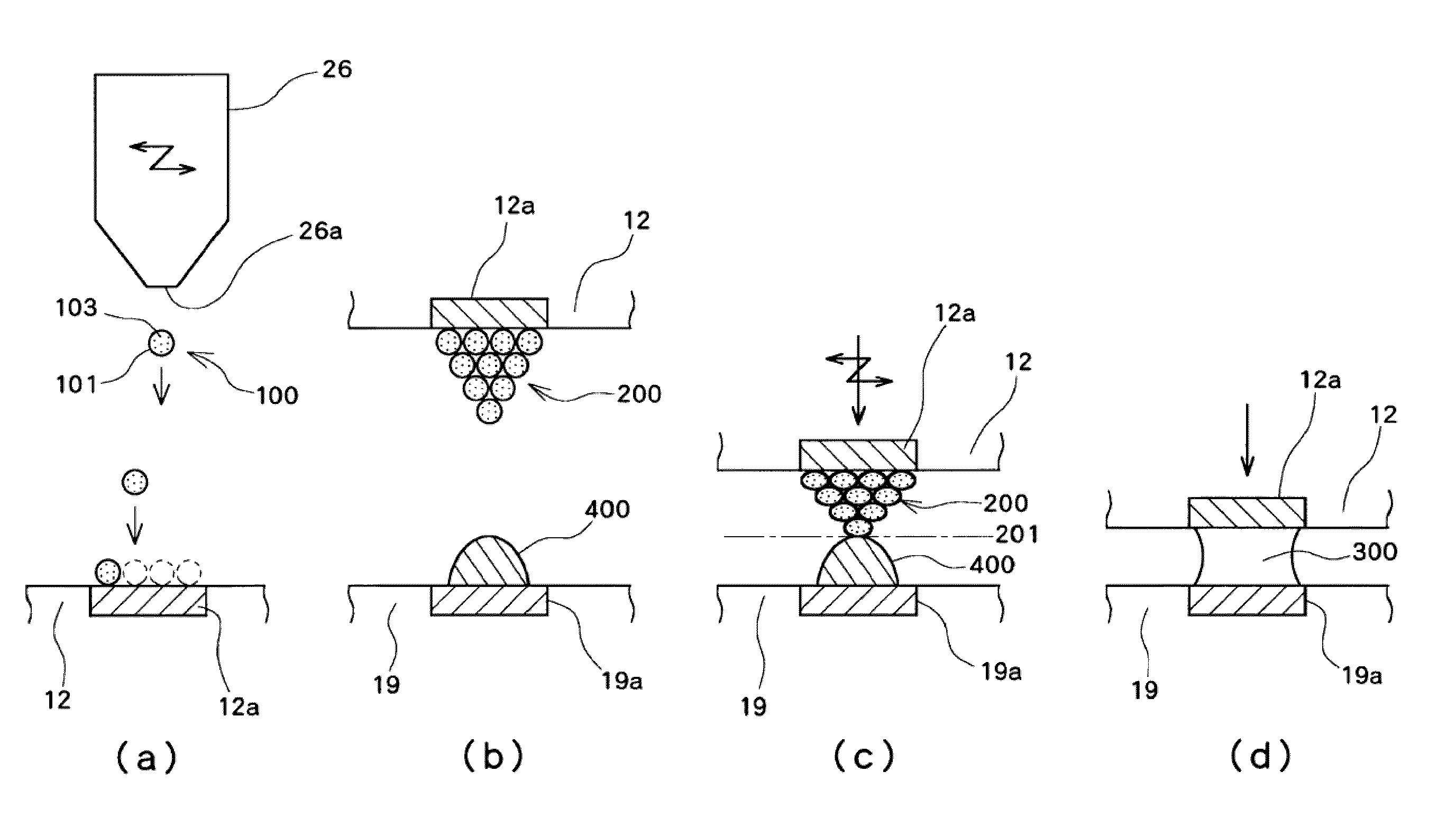
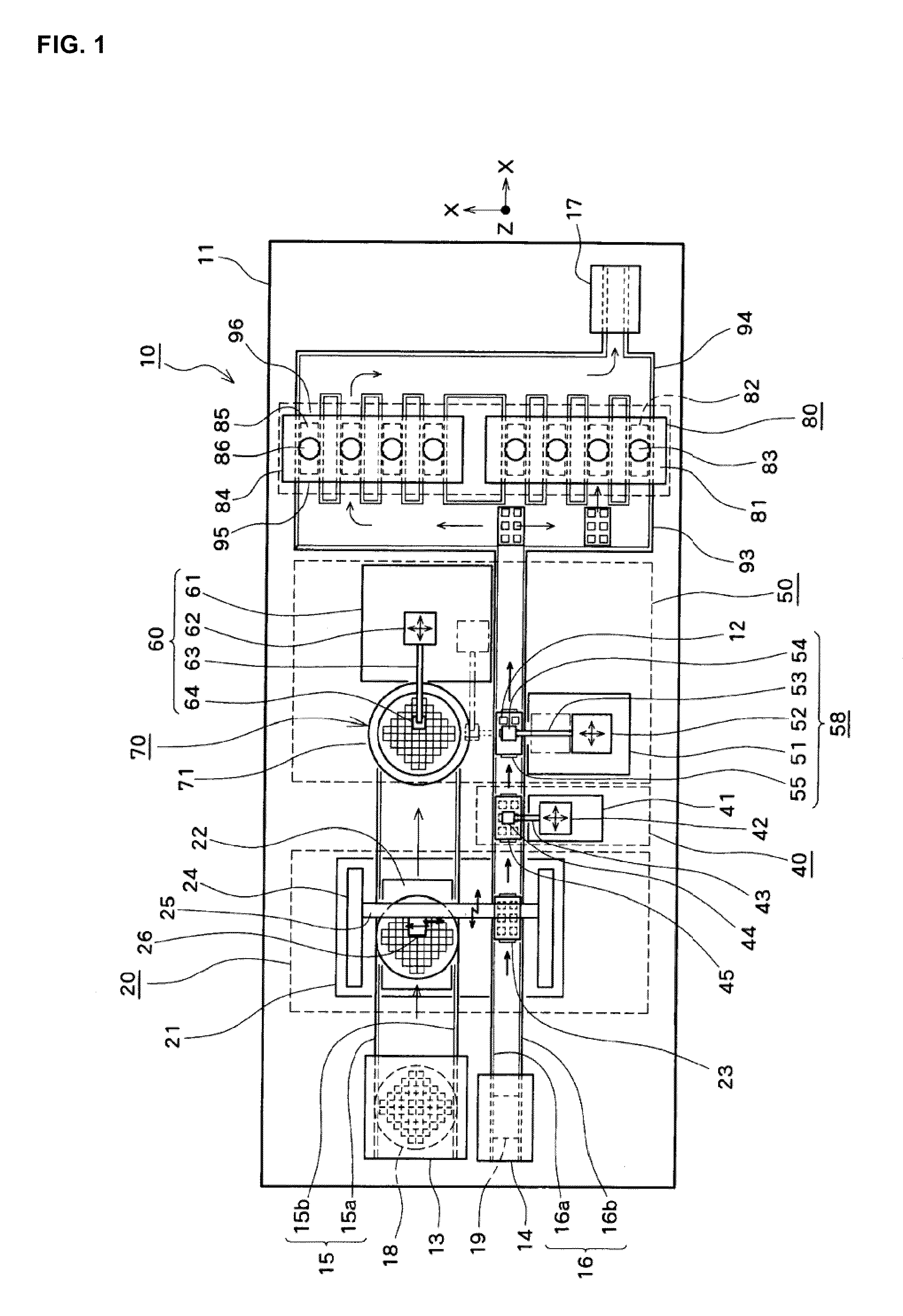
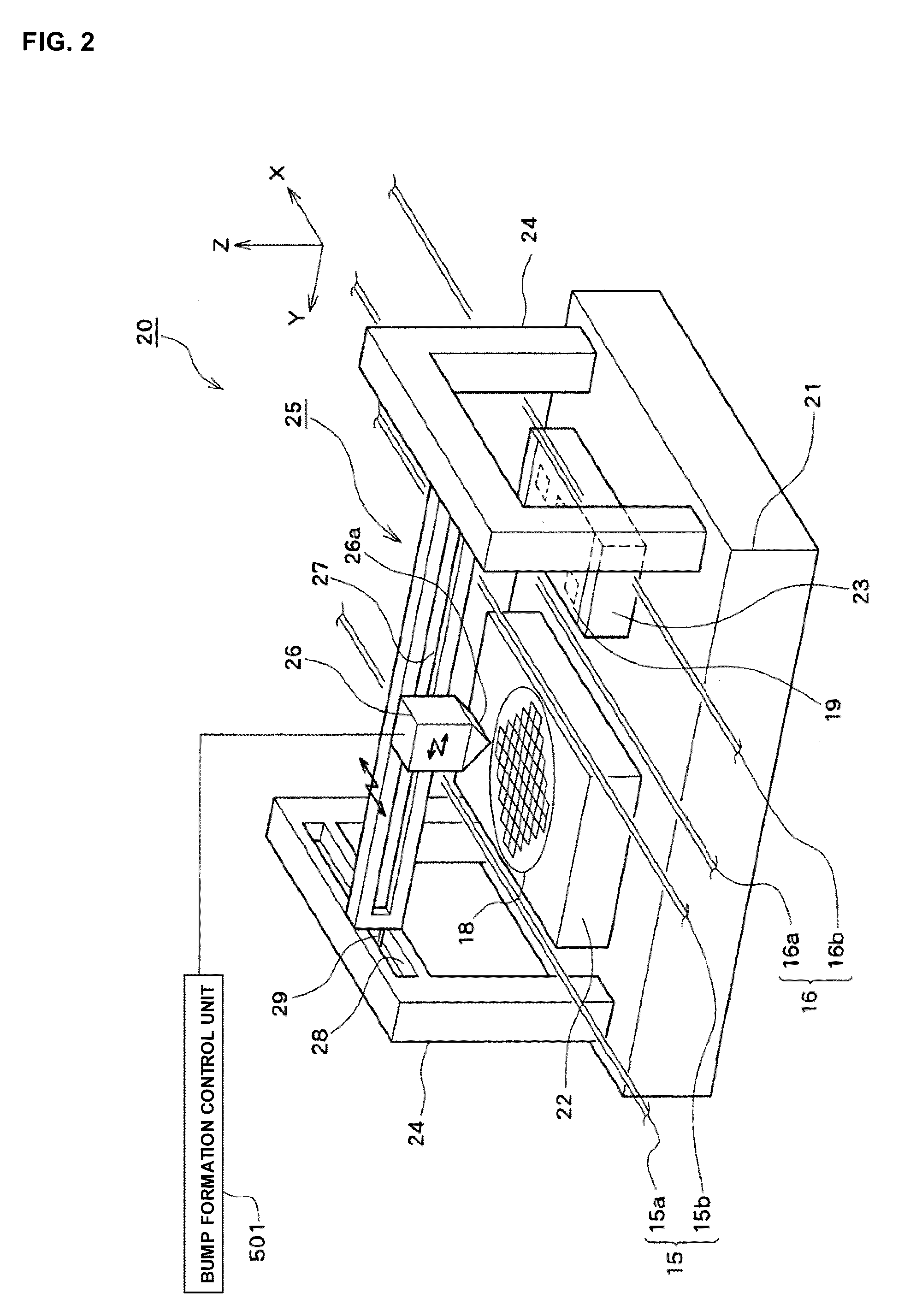
[0044]The following describes an exemplary embodiment according to the present invention with reference to the drawings. As shown in FIG. 1, a bonding apparatus 10 according to this exemplary embodiment is provided with a bump formation mechanism 20 disposed in a frame 11, an underfill material application mechanism 40, a primary bonding mechanism 50, and a secondary bonding mechanism 80. The secondary bonding mechanism 80 is provided with two pressure heating furnaces which are a first pressure heating furnace 81 and a second pressure heating furnace 84. A wafer magazine 13 that feeds a wafer 18 and a substrate magazine 14 that feeds a circuit board 19 are provided on a workpiece feeding side which is on a left side of the bonding apparatus 10 in FIG. 1, and a product magazine 17 that stores a finished product is provided on a product carry-out side which is on a right side of the bonding apparatus 10 in FIG. 1. The wafer magazine 13, a bump formation mechanism 20, and the primary ...


PUM

PropertyMeasurementUnit
Temperatureaaaaaaaaaa
Forceaaaaaaaaaa

Abstract

A bonding apparatus (10) that bonds an electrode of a semiconductor die (12) and an electrode of a circuit board (19) using a metal nano paste includes a bump formation mechanism (20) that forms bump by injecting microdroplets of a metal nano paste on each electrode, a primary bonding mechanism (50) that carries out primary bonding to the electrodes in a non-conductive state by pressing the bump of the semiconductor die (12) against the bump of the circuit board (19), and a secondary bonding mechanism (80) that carries out secondary bonding so that the electrodes become conductive by pressurizing the primary bonded bump in bonding direction and by heating the bump to pressurize and sinter the metal nanoparticles in the bump. With this, it is possible to efficiently bond the electrodes with a simple and easy way while reducing a bonding load.

Description

TECHNICAL FIELD[0001]The present invention relates to bonding apparatuses and methods of bonding electrodes using a metal nano paste.BACKGROUND ART[0002]A method for bonding an electrode of an electronic component such as a semiconductor die, and an electrode in a circuit pattern on a circuit board is described in Japanese Patent Application Publication No. H09-326416 through the formation of a solder bump on an electrode pad of the electronic component, positioning the electronic component such that the formed solder bump faces down toward the electrode on the circuit board, and heating the solder bump, thereby bonding the electrodes. A method for bonding an electrode of an electronic component is also described in Japanese Patent Application Publication No. H10-150075. This publication describes a flip-chip bonding method of applying an electrically conductive bonding agent over a surface of a gold bump formed on an electrode surface of an electronic component such as a semiconduc...

Claims


Application Information

Patent Timeline
IPC IPC(8): H01L21/822H01L21/60B23K3/06B23K1/06B23K20/10
CPCB23K1/0016H01L2224/1131B23K2201/40H01L21/67144H01L24/11H01L24/16H01L24/81H01L24/94H01L25/50H01L2224/13099H01L2224/13139H01L2224/13144H01L2224/13147H01L2224/274H01L2224/75H01L2224/7525H01L2224/75744H01L2224/75745H01L2224/7598H01L2224/81121H01L2224/81205H01L2224/8121H01L2224/81815H01L2224/8184H01L2924/01013H01L2924/01027H01L2924/01029H01L2924/01033H01L2924/0104H01L2924/01046H01L2924/01047H01L2924/01078H01L2924/01079H01L2924/01082H01L2924/14H01L24/13H01L2224/16145H01L2924/01005H01L2924/01006H01L2924/01024H01L2924/014B23K3/0623B23K2101/40H01L2924/351H01L24/75H01L2224/11332H01L2224/11318H01L2224/0557H01L2224/05573H01L2224/056H01L2224/05571H01L2924/00014H01L2224/0554H01L2924/00H01L2224/05599H01L2224/0555H01L2224/0556H01L23/12B82Y30/00
Inventor MAEDA, TORU
Owner SHINKAWA CO LTD
Why Eureka
Try Eureka