Electric contact and method for producing the same and connector using the electric contacts

a technology of electric contacts and printed circuit boards, which is applied in the direction of manufacturing tools, non-printed masks, etching metal masks, etc., can solve the problems of short circuit, defective or failed electrical connections, and difficulty in accurately aligning the holes worked from the opposite sides

Inactive Publication Date: 2010-04-22
OHTSUKI TOMONARI +4
View PDF5 Cites 22 Cited by
  • Summary
  • Abstract
  • Description
  • Claims
  • Application Information

AI Technical Summary

Benefits of technology

[0040]In view of the problems of the prior art described above, it is a further object of the invention to provide electric contact structures which permit a large amount of electric current to flow therein and are adapted to contact a mating object in an optimized manner without increasing manufacturing cost,
[0136]Consequently, slits can be easily formed, which have a width W less than and a length L large than the focused beam diameter D.

Problems solved by technology

On proceeding of narrower pitches of electric contacts, however, when contacts having a certain height are formed, the diameter of the contacts becomes larger in comparison with the narrow pitch so that the contacts are arranged in close proximity to one another, thereby resulting into defective or failed electrical connection and causing short circuit.
The holes worked from the opposite sides are difficult to be accurately aligned with each other so that they tend to be staggered.
Consequently, it is difficult to obtain a concentric through-hole with high positional accuracy using this prior art method.
Therefore, this method is not suitable for machining a great many through-holes and tends to increase the manufacturing cost.
In this way, it is difficult to obtain through-holes each consisting of accurately aligned halves, and through-holes with high positional accuracy.
On proceeding of narrower pitches of electric contacts in recent years, however, when contacts of a certain height are formed, the diameter of the electric contacts becomes larger in comparison with the narrow pitch so that the electric contacts are in close proximity to one another, thereby causing defective or failed electrical connection and short circuit as described above.
Even if the contacts are spaced apart from one another as much as possible to avoid such problems, the height of the contacts must necessarily be lowered so that even required predetermined height cannot be ensured.
With the electric contacts each arranged on a copper foil of the flexible printed circuit board as disclosed in the Patent Literatures 2 and 3, on the other hand, there is a problem that a large amount of electric current could not be employed due to the thin copper foils.
If thick copper foils are used, a large amount of current could be employed, but it would provide an impediment to the flexibility of the circuit board.
Moreover, when an electric contact as disclosed in the Patent Literature 2 or 3 is arranged on a copper foil of a flexible printed circuit board, as adherence between the copper plate layer and the cover lay is poor, a particular treatment for the cover lay will be needed, which is tedious and time-consuming, resulting in increased manufacturing cost.
However, the wet lubrication is likely to cause dust or dirt accumulation, resulting in defective or failed connection, and is gradually being dried over time to become poor in lubricating ability.
However, the dry lubrication (diamond-like carbon coating) is poor in conductivity, although superior in wear-resistance.
If such holes could not be formed perpendicularly to surfaces of a plate to be formed with the holes, insertion of the conductors into the holes becomes difficult and hence vertically holding the conductors becomes impossible, resulting in defective or failed connection and obstruction of miniaturization of the appliances and connectors.
However, the laser beam machining or drilling could not form a number of holes at a time, and hence has to form a number of holes one after another, resulting in increased manufacturing cost.
In drilling, chisel edges at the tip of a drill will adversely affect resulting fine holes.
In more detail, the chisel edges tend to wobble under the influence of even slight flaws or scratches or unevenness of the surface so that the starting position of the hole would be shifted from the target position and formation of a vertical hole perpendicular to the surface would become impossible.
Although a fine hole perpendicular to the surfaces can be formed using the laser beam machining, its manufacturing cost would go up for the reason described above and due to high expense of the method itself.
However, both the methods could not cut a slit, such as a U-shaped slit, of a width less than 30 μm.

Method used


Image

  • Electric contact and method for producing the same and connector using the electric contacts
  • Electric contact and method for producing the same and connector using the electric contacts
  • Electric contact and method for producing the same and connector using the electric contacts

Examples


Embodiment Construction

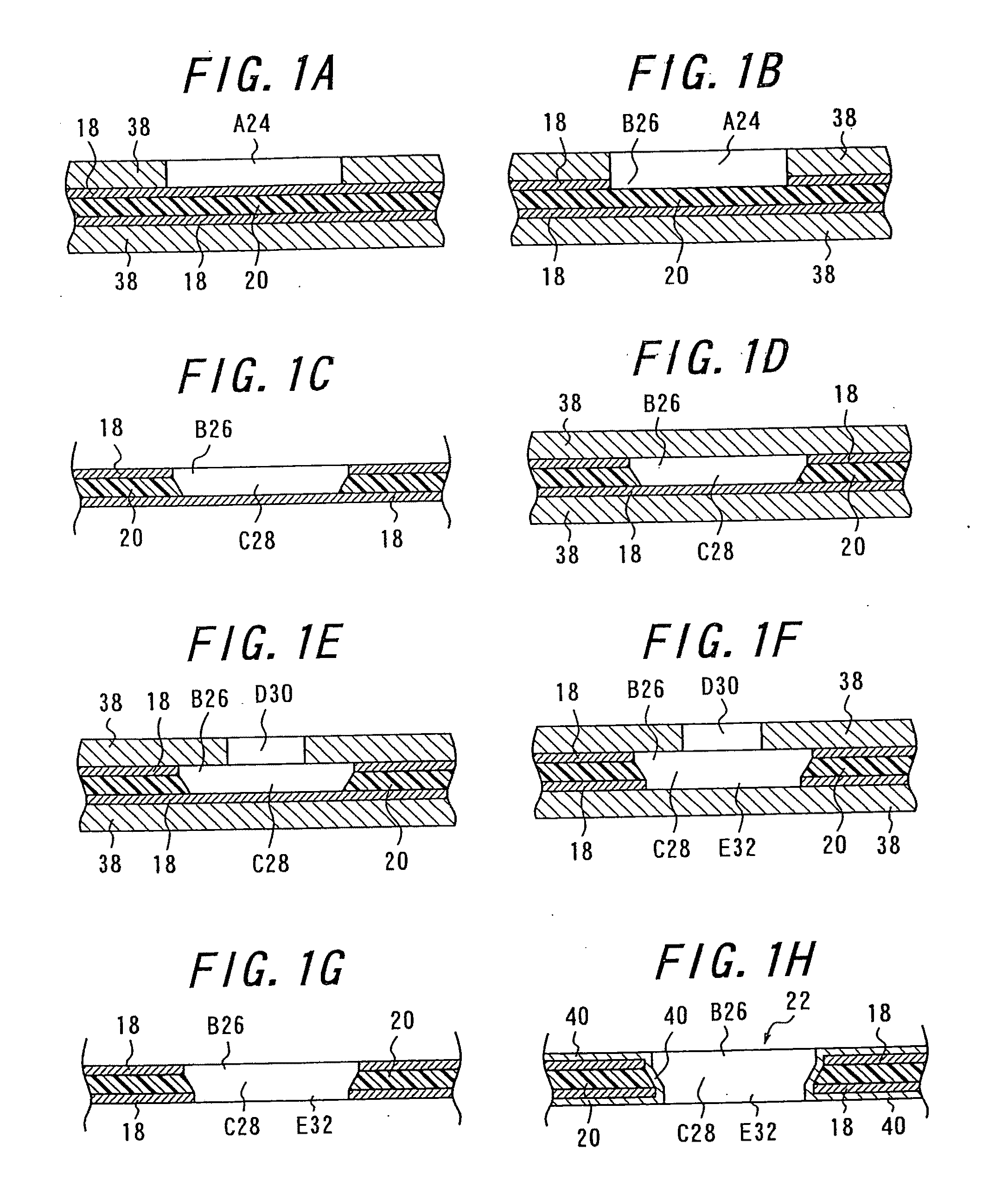
[0184]First, the production method of the through hole of claim 1 will be explained.

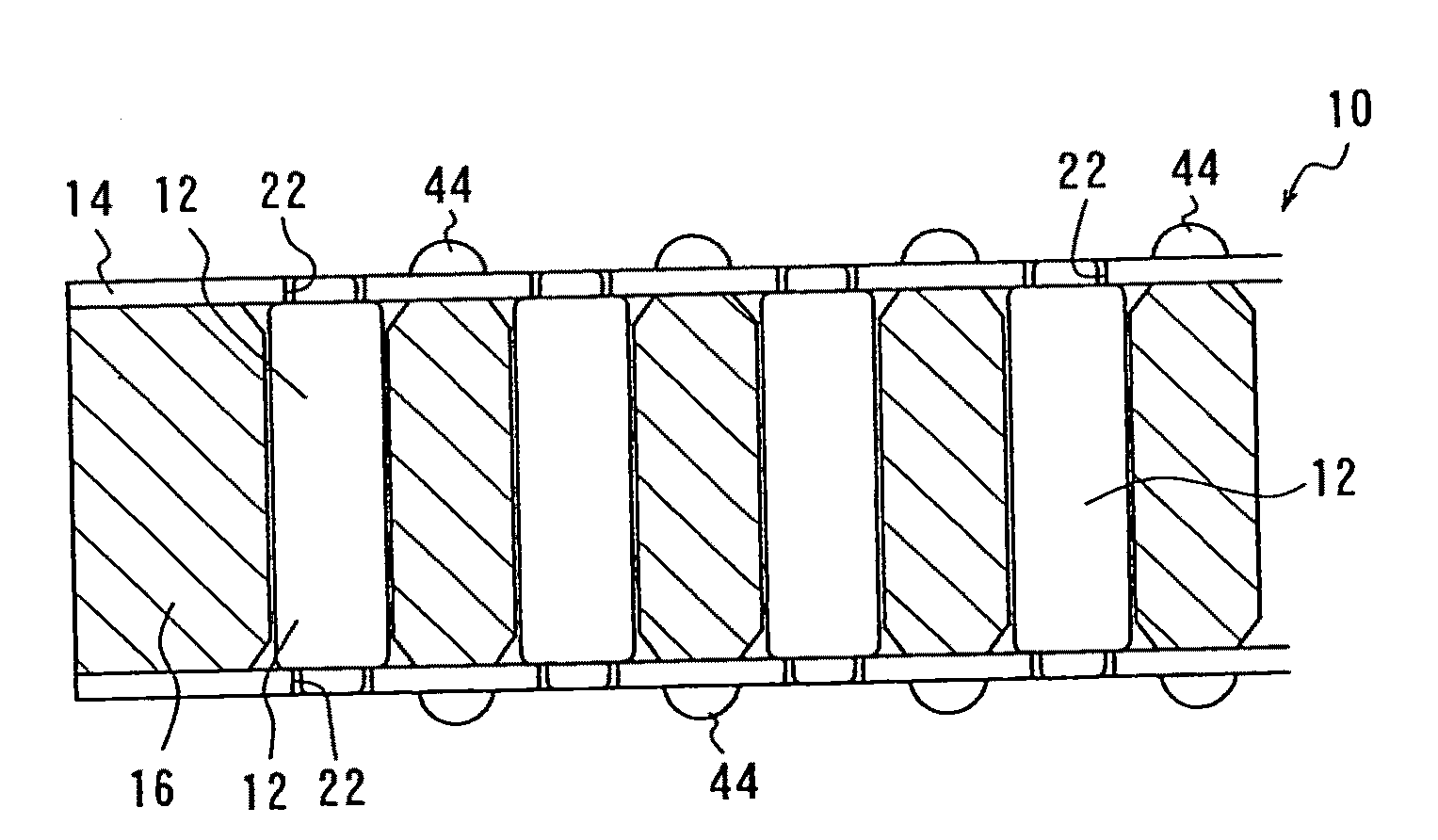
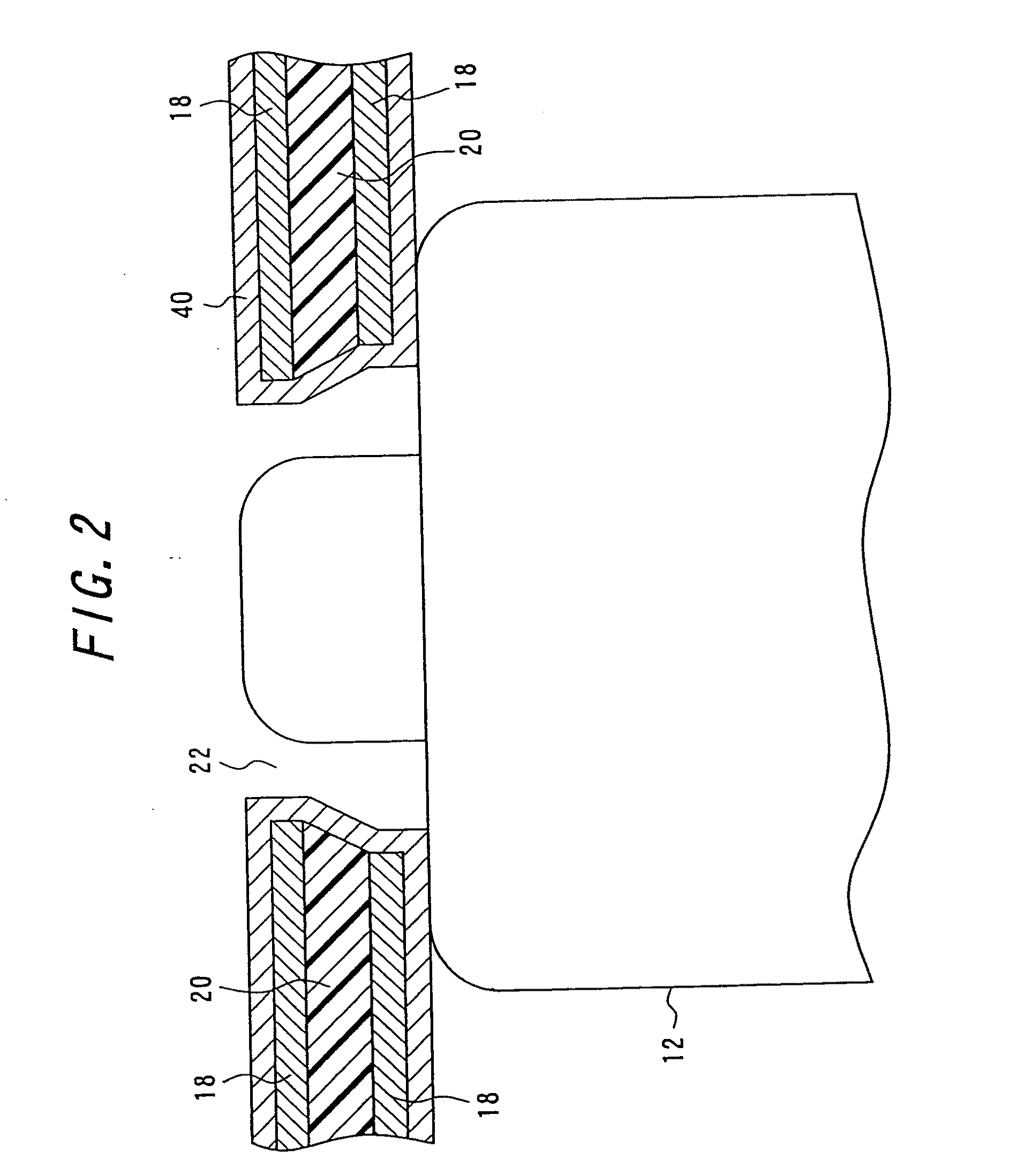
[0185]The method for producing a board formed with through-holes 22 according to the invention will be explained with reference to FIGS. 1A to 1H. FIGS. 1A to 1H are drawings for explaining the method for producing the board formed with the through-holes. The method for producing the board formed with the through-holes 22 is carried out in the following steps in which a flexible printed circuit board 14 consisting of a polyimide layer 20 and copper foils 18 and is worked in one direction from its one surface.

[0186]In the first step, as shown in FIG. 1A an acid proof material layer 38 having a plurality of holes A24 each having a required diameter and located at a predetermined position is formed by printing on one surface of the board 14, or an acid proof film is attached to the one surface, and an acid proof material layer 38 is formed by printing on the whole other surface of the board 14, or an ac...


PUM

PropertyMeasurementUnit
current densityaaaaaaaaaa
widthaaaaaaaaaa
widthaaaaaaaaaa

Abstract

A board consisting of a polyimide layer and copper foils is worked from one direction by etching to form through-holes, and the copper foils and inside of the through-holes are plated with copper, or the board is worked by etching or laser machining to form blind holes to expose the copper foils on the other side and through-holes simultaneously, and copper foils and insides of the blind holes and the through-holes are plated with copper. A metal ball plated with a noble metal is fixed on the copper foil by solidification of a metal paste to form an electric contact. Two superimposed plastic sheets are formed with holes each having a projection on inner wall of the hole, thereby vertically holding conductors by the projections of the holes of the superimposed plastic sheets. A laser beam machining method fabricates grooves or slits in a workpiece.

Description

BACKGROUND OF THE INVENTION[0001]This invention relates to a method for producing a flexible printed circuit board formed with a plurality of through-holes, and more particularly to electric contacts and methods for producing the electric contacts whose heights are uniform and as high as possible without increasing their diameters, and further to electric contacts each having a shape adapted to that of a mating object, or having a wear resistant conductive hard film on a portion adapted to contact a mating object, or each comprising copper foils on both sides of a board and adapted to be electrically connected to each other. The invention further relates to a structure for vertically holding conductors in the form of a pin, a method for producing plastic sheets for use in the structure, and a laser beam machining method for forming slits having a width less than and a length larger than a focused laser beam diameter, and more particularly to connectors using the structure and utiliz...

Claims


Application Information

Patent Timeline
Patent Type & Authority Applications(United States)
IPC IPC(8): H05K1/00
CPCB23K26/0661Y10T29/49224C25D5/10H01L24/03H01L24/05H01L2224/0401H01L2924/01004H01L2924/01005H01L2924/01013H01L2924/01014H01L2924/01015H01L2924/01028H01L2924/01029H01L2924/01074H01L2924/01078H01L2924/01079H01L2924/014H01L2924/14H01L2924/19041H01L2924/3011H05K1/0346H05K1/0393H05K3/002H05K3/0032H05K3/061H05K3/321H05K3/326H05K3/368H05K3/4015H05K3/42H05K2201/0367H05K2201/0373H05K2201/09081H05K2201/091H05K2201/09472H05K2201/09509H05K2201/09827H05K2201/10234H05K2201/10303H05K2201/10424H05K2203/0554H05K2203/0557H05K2203/0789H05K2203/0793H01L2924/01006H01L2924/01033H01L2224/05552C25D5/022Y10T29/49165H01L2224/05001H01L2224/0554H01L2924/00012C25D5/12
Inventor OHTSUKI, TOMONARIYAMAZAKI, YASUEDAIMON, HIROFUMIMATSUO, KOZOTAKAMI, SACHI
Owner OHTSUKI TOMONARI
Why Eureka
Try Eureka