Image processing method of optical navigator and optical navigator using the same
- Summary
- Abstract
- Description
- Claims
- Application Information
AI Technical Summary
Benefits of technology
Problems solved by technology
Method used
Image
Examples
Embodiment Construction
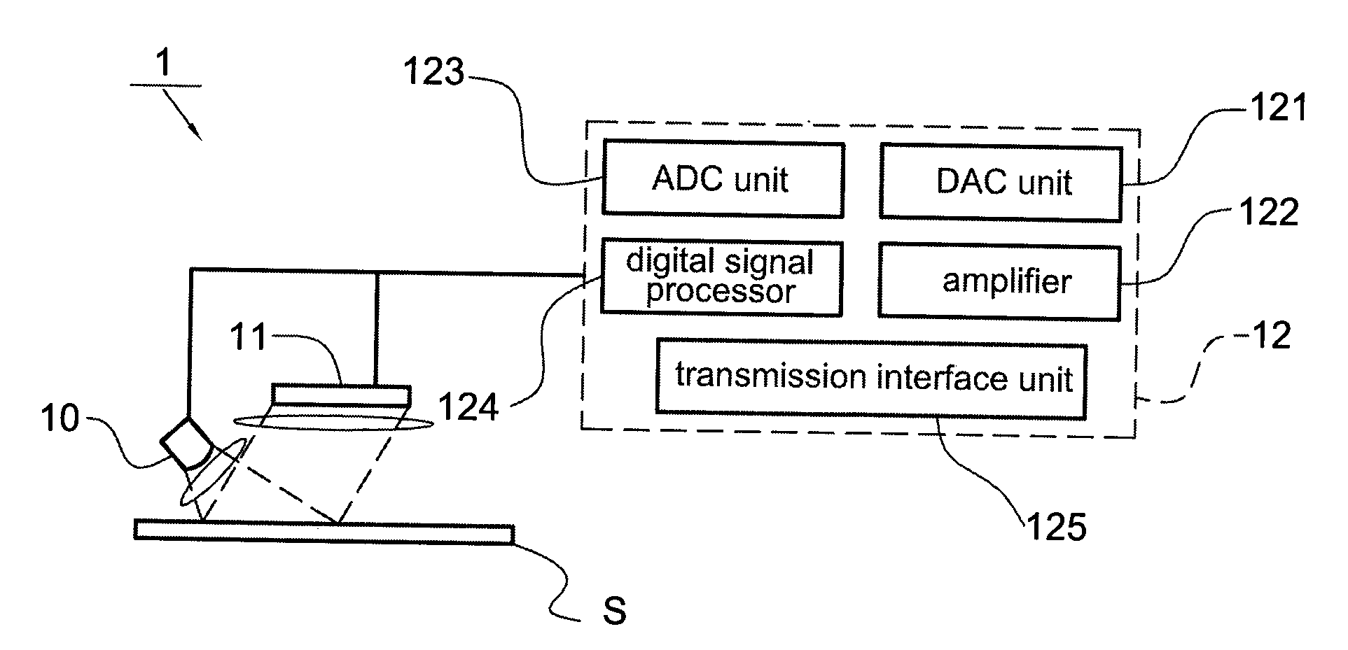
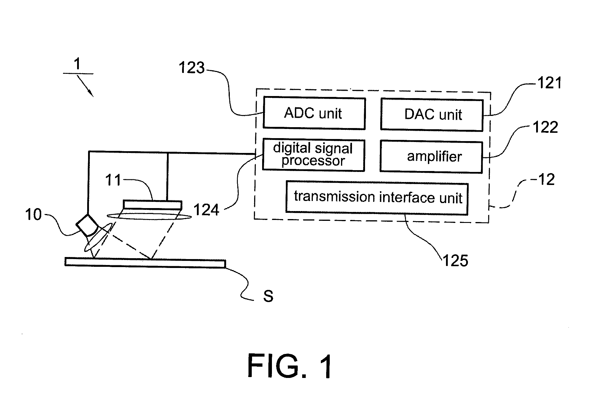
[0028]Please refer to FIG. 1, it shows a schematic diagram of the optical navigator 1 according to one embodiment of the present invention. The optical navigator 1 includes a light source 10, an image sensor 11 and an image processing unit 12. Embodiments of the light source 10 include a light emitting diode and a laser diode. The light source 10 is for lighting a work surface “S”, e.g. the surface of a table or the surface of a mouse pad. Embodiments of the image sensor 11 include a charge-coupled device (CCD) image sensor and a complementary-metal-oxide semiconductor (CMOS) image sensor. The image sensor 11 is for sensing the reflected light from the work surface “S” to form a two-dimensional analog image. The two-dimensional analog image is an image composed of the brightness sensed by each pixel of the image sensor 11. The image processing unit 12 is coupled to the light source 10 and the image sensor 11 for processing images captured by the image sensor 11 and for controlling t...
PUM
 Abstract
Description
Claims
Application Information


