Organic light emitting diode display

a light-emitting diode and organic technology, applied in the field of organic light-emitting diodes (oled) displays, can solve the problems of low light-emitting efficiency, high power consumption, and low luminan

Active Publication Date: 2010-04-29
LG DISPLAY CO LTD
View PDF2 Cites 86 Cited by
  • Summary
  • Abstract
  • Description
  • Claims
  • Application Information

AI Technical Summary

Benefits of technology

[0012]Embodiments of the invention provide an organic light emitting diode (OLED) display capable of monitoring defects su

Problems solved by technology

However, the PDP has disadvantages such as low light emitting efficiency, low luminance, and high power consumption.
However, because the TFT LCD is not a self-emission display, the TFT LCD has a narrow viewing angle and a low response speed.
Even if a display panel of the OLED display is damaged, the OLED display may partially emit light because of a normal operation of the driver IC.
As described above, if only the non-damage portion of th

Method used


Image

  • Organic light emitting diode display
  • Organic light emitting diode display
  • Organic light emitting diode display

Examples


first exemplary embodiment

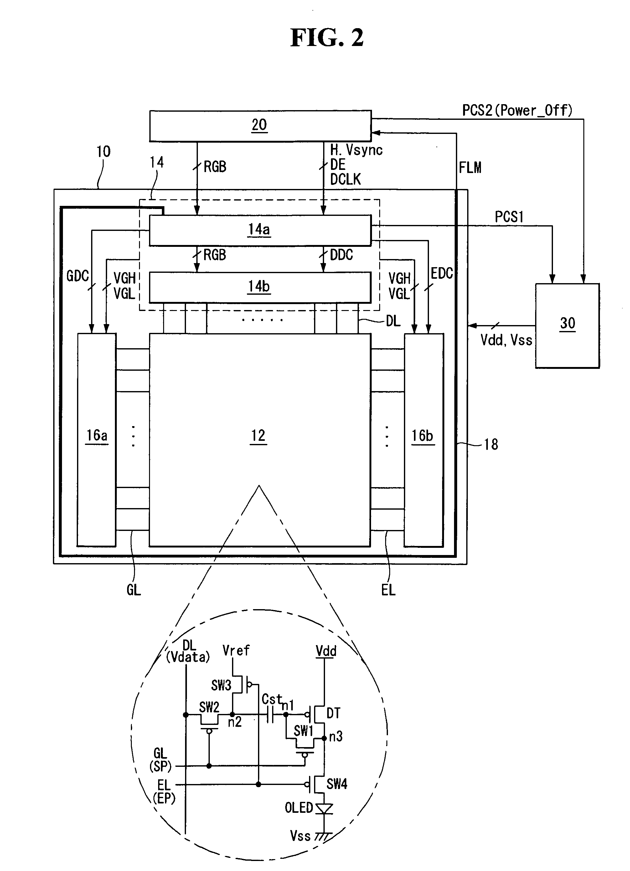
[0028]FIG. 2 is a block view of an organic light emitting diode (OLED) display according to a first exemplary embodiment of the invention.

[0029]As shown in FIG. 2, the OLED display according to the first exemplary embodiment of the invention includes a display panel 10, a system 20, and a power integrated circuit (IC) 30. A driver IC 14 is mounted in a non-display area of the display panel 10 using a chip-on-glass (COG) technology, and a scan driver 16a and an emission driver 16b are formed in the non-display area of the display panel 10 using a gate-in-panel (GIP) technology.

[0030]A plurality of data lines DL, a plurality of gate lines GL, and a plurality of emission lines EL cross one another in an effective display area of the display panel 10, and a pixel 12 is formed at each of crossings of the lines DL, GL, and EL in a matrix format. Each of the pixels 12 includes an organic light emitting diode, a driving thin film transistor (TFT), a plurality of switching TFTs, and a storag...

second exemplary embodiment

[0041]FIG. 6 is a block view of an OLED display according to a second exemplary embodiment of the invention.

[0042]As shown in FIG. 6, the OLED display according to the second exemplary embodiment of the invention includes a display panel 110, a system 120, and a power IC 130. A driver IC 114 is mounted in a non-display area of the display panel 110 using a COG technology, and a scan driver 116a and an emission driver 116b are formed in the non-display area of the display panel 110 using a GIP technology.

[0043]In the OLED display according to the second exemplary embodiment of the invention, a timing controller 114a continuously monitors a FLM signal from a monitoring signal line 118 and generates a second power control signal PCS2 based on a monitoring result. On the other hand, in the OLED display according to the first exemplary embodiment of the invention, the system 20 continuously monitors the FLM signal from the monitoring signal line 18 and generates the second power control ...

third exemplary embodiment

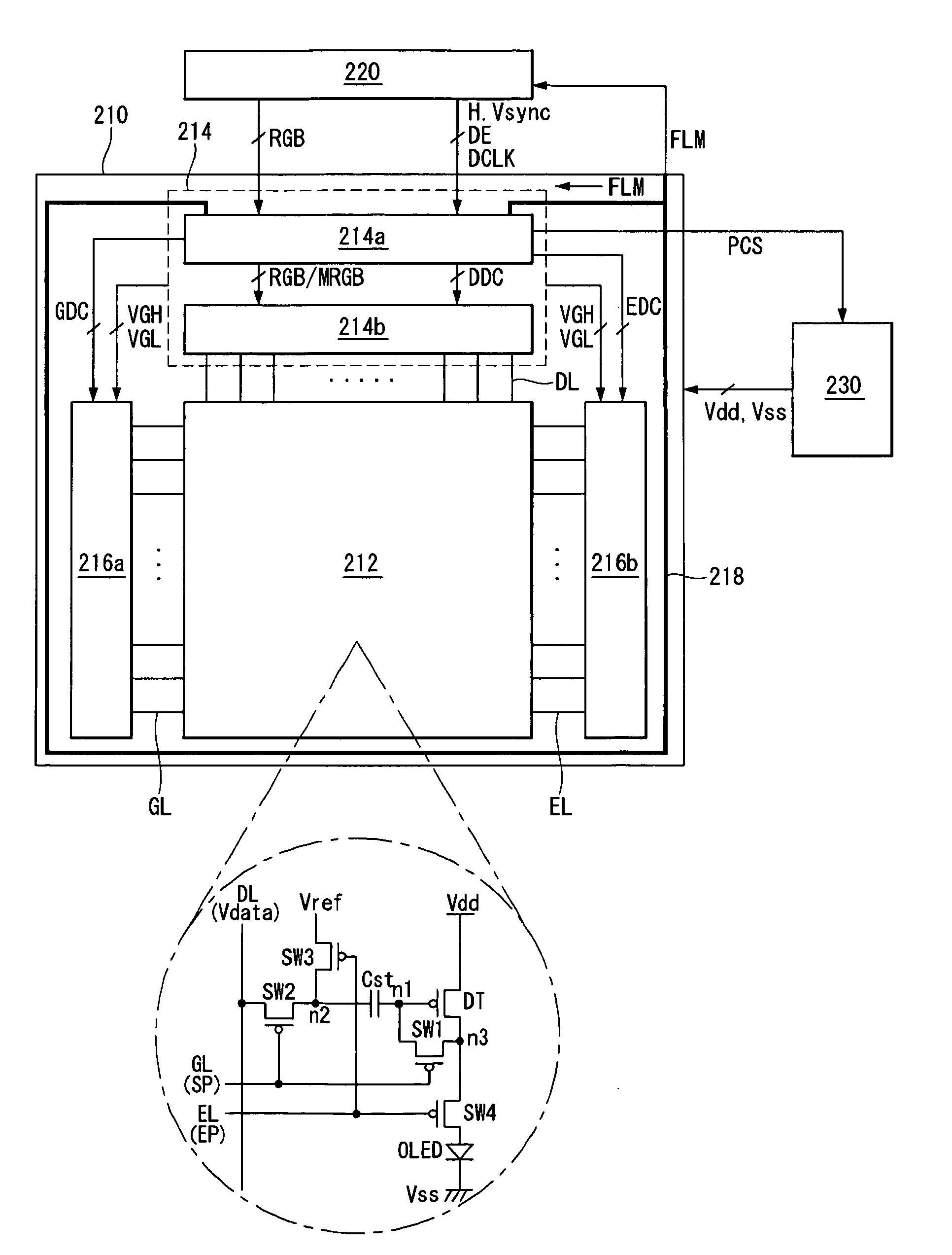
[0044]FIG. 7 is a block view of an OLED display according to a third exemplary embodiment of the invention.

[0045]As shown in FIG. 7, the OLED display according to the third exemplary embodiment of the invention includes a display panel 210, a system 220, and a power IC 230. A driver IC 214 is mounted in a non-display area of the display panel 210 using a COG technology, and a scan driver 216a and an emission driver 216b are formed in the non-display area of the display panel 210 using a GIP technology. The display panel 210, the system 220, the scan driver 216a, and the emission driver 216b in the third exemplary embodiment are substantially the same as the display panel 110, the system 120, the scan driver 116a, and the emission driver 116b in the second exemplary embodiment, respectively. The power IC 230 is substantially the same as the configuration of the power IC 130 in the second exemplary embodiment except determining whether or not the power IC 230 supplies driving voltages...


PUM


Abstract

An organic light emitting diode (OLED) display is provided. The OLED display includes a display panel including pixels formed at each of crossings of a plurality of gate lines and a plurality of data lines, a monitoring signal line formed along an outer area of the display panel, a first signal supply unit that supplies a monitoring signal to the monitoring signal line and generates a first power control signal, a power supply unit that supplies a high potential driving voltage and a low potential driving voltage to the pixels, and a second signal supply unit that monitors the monitoring signal and generates a second power control signal. If the monitoring signal is not monitored, the second signal supply unit controls the power supply unit through the second power control signal and allows the power supply unit to stop supplying one of the high and low potential driving voltages to the pixels.

Description

[0001]This application claims the benefit of Korea Patent Application No. 10-2008-106155 filed on Oct. 28, 2008, the entire contents of which is incorporated herein by reference for all purposes as if fully set forth herein.BACKGROUND OF THE INVENTION[0002]1. Field of the Invention[0003]Embodiments of the invention relate to an organic light emitting diode (OLED) display capable of preventing a local light emission due to a damage of a display panel.[0004]2. Discussion of the Related Art[0005]Various flat panel displays whose weight and size are smaller than cathode ray tubes have been recently developed. Examples of the flat panel displays include a liquid crystal display (LCD), a field emission display (FED), a plasma display panel (PDP), and an electroluminescence device.[0006]Because the PDP has a simple structure and is manufactured through a simple process, the PDP has been considered as a display device having characteristics such as lightness in weight and thin profile and p...

Claims


Application Information

Patent Timeline
IPC IPC(8): G06F3/038
CPCG09G2320/043G09G2330/02G09G2330/022G09G2330/045G09G2300/0861G09G3/006G09G3/3233G09G2300/0819G09G2300/0842G09G2330/10G09G2360/18
Inventor JEON, CHANGHOONKIM, KEUNCHOUL
Owner LG DISPLAY CO LTD
Why Eureka
Try Eureka